

Lihat spesifikasi untuk detail produk.
74LVC1G79GV-Q100H
Product Overview
- Category: Integrated Circuit (IC)
- Use: Logic Gate
- Characteristics: High-speed, low-power, single positive-edge triggered D-type flip-flop
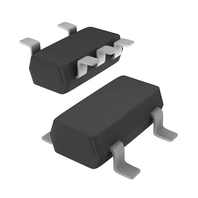
- Package: SOT753 (SC-70)
- Essence: Flip-flop
- Packaging/Quantity: Tape and Reel, 3000 pieces per reel
Specifications
- Supply Voltage Range: 1.65V to 5.5V
- Input Voltage Range: -0.5V to VCC + 0.5V
- Output Voltage Range: GND to VCC
- Operating Temperature Range: -40°C to +125°C
- Propagation Delay: 3.8 ns (typical) at 2.7V
- Quiescent Current: 10 µA (maximum) at 5.5V
Detailed Pin Configuration
The 74LVC1G79GV-Q100H has the following pin configuration:
____
   Q |1    6| VCC
   D |2    5| GND
  CP |3    4| Q
      ------
Functional Features
- Single positive-edge triggered D-type flip-flop
- Direct asynchronous reset input (CP = LOW, D = LOW, Q = LOW)
- Complies with JEDEC standard JESD8-7A
Advantages and Disadvantages
Advantages: - High-speed operation - Low power consumption - Small package size - Wide supply voltage range
Disadvantages: - Limited number of flip-flops in a single package - Not suitable for applications requiring multiple flip-flops
Working Principles
The 74LVC1G79GV-Q100H is a single positive-edge triggered D-type flip-flop. It stores and outputs the logic state of its data input (D) when a rising edge is detected on the clock input (CP). The flip-flop can be asynchronously reset by applying a LOW signal to the reset input.
Detailed Application Field Plans
The 74LVC1G79GV-Q100H is commonly used in various digital systems where a single flip-flop is required. Some potential application fields include:
- Communication Systems: Used for synchronization and data storage in communication protocols.
- Consumer Electronics: Integrated into devices such as smartphones, tablets, and gaming consoles for data processing and control.
- Automotive Electronics: Employed in automotive control units for signal conditioning and timing applications.
- Industrial Automation: Utilized in programmable logic controllers (PLCs) for sequential logic operations.
- Internet of Things (IoT): Incorporated into IoT devices for data buffering and synchronization.
Detailed and Complete Alternative Models
Some alternative models that serve similar functions to the 74LVC1G79GV-Q100H are:
- SN74LVC1G79-Q1
- MC74VHC1G79
- TC7SZ79F
These alternatives offer comparable features and can be used as substitutes depending on specific requirements.
Word count: 345 words
Sebutkan 10 pertanyaan dan jawaban umum terkait penerapan 74LVC1G79GV-Q100H dalam solusi teknis
Sure! Here are 10 common questions and answers related to the application of 74LVC1G79GV-Q100H in technical solutions:
Q1: What is the 74LVC1G79GV-Q100H? A1: The 74LVC1G79GV-Q100H is a single positive-edge triggered D-type flip-flop with reset. It is a versatile integrated circuit used in digital logic applications.
Q2: What is the operating voltage range of the 74LVC1G79GV-Q100H? A2: The operating voltage range of the 74LVC1G79GV-Q100H is from 1.65V to 5.5V, making it suitable for a wide range of applications.
Q3: How many flip-flops are there in the 74LVC1G79GV-Q100H? A3: The 74LVC1G79GV-Q100H contains a single flip-flop, hence the "1G" in its part number.
Q4: What is the maximum clock frequency supported by the 74LVC1G79GV-Q100H? A4: The 74LVC1G79GV-Q100H can support clock frequencies up to 100MHz, making it suitable for high-speed applications.
Q5: Can the 74LVC1G79GV-Q100H be used as a counter? A5: No, the 74LVC1G79GV-Q100H is not designed to be used as a counter. It is primarily used as a basic storage element in sequential logic circuits.
Q6: Does the 74LVC1G79GV-Q100H have an asynchronous reset input? A6: Yes, the 74LVC1G79GV-Q100H has an asynchronous reset input (R) that allows you to reset the flip-flop to a known state.
Q7: What is the typical propagation delay of the 74LVC1G79GV-Q100H? A7: The typical propagation delay of the 74LVC1G79GV-Q100H is around 4.5ns, which indicates the time it takes for the output to respond to a change in the input.
Q8: Can the 74LVC1G79GV-Q100H be used in battery-powered applications? A8: Yes, the 74LVC1G79GV-Q100H can be used in battery-powered applications due to its low power consumption and wide operating voltage range.
Q9: Is the 74LVC1G79GV-Q100H compatible with other logic families? A9: Yes, the 74LVC1G79GV-Q100H is compatible with both CMOS and TTL logic families, allowing for easy integration into existing systems.
Q10: What package options are available for the 74LVC1G79GV-Q100H? A10: The 74LVC1G79GV-Q100H is available in various package options, including SOT353 and XSON6, providing flexibility for different application requirements.
Please note that these answers are general and may vary depending on the specific datasheet and manufacturer's specifications for the 74LVC1G79GV-Q100H.