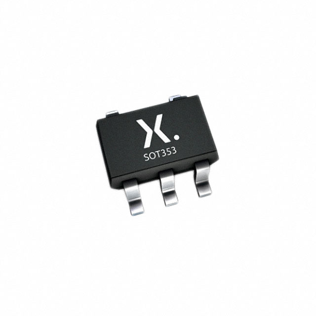
Lihat spesifikasi untuk detail produk.

74LVC1G125GW-Q100
Basic Information Overview
- Category: Integrated Circuit (IC)
- Use: Buffer/Driver
- Characteristics: Low-voltage, single gate, non-inverting buffer/driver
- Package: SOT753 (SC-70)
- Essence: This IC is designed to provide a high-speed, low-power solution for buffering or driving signals in various electronic applications.
- Packaging/Quantity: Available in tape and reel packaging with 3000 units per reel.
Specifications
- Supply Voltage Range: 1.65V to 5.5V
- High-Level Input Voltage: 0.7 x VCC
- Low-Level Input Voltage: 0.3 x VCC
- Output Drive Capability: ±24mA
- Propagation Delay: 4.3ns (typical)
- Operating Temperature Range: -40°C to +125°C
Detailed Pin Configuration
The 74LVC1G125GW-Q100 IC has the following pin configuration:
____
   Y1 |    | VCC
   A  |    | Y2
 GND  |____| OE
Functional Features
- Non-inverting buffer/driver: The IC provides a non-inverted output signal compared to the input signal.
- Wide supply voltage range: It can operate within a wide range of supply voltages from 1.65V to 5.5V.
- High-speed operation: The propagation delay of the IC is typically 4.3ns, making it suitable for high-speed applications.
- Low power consumption: The IC is designed to consume minimal power, making it energy-efficient.
Advantages and Disadvantages
Advantages: - Wide supply voltage range allows compatibility with various systems. - High-speed operation enables efficient signal buffering and driving. - Low power consumption helps in reducing overall power requirements.
Disadvantages: - Limited output drive capability may not be suitable for applications requiring higher current levels. - Single gate configuration restricts the number of signals that can be buffered or driven simultaneously.
Working Principles
The 74LVC1G125GW-Q100 is a single gate buffer/driver IC. It takes an input signal and provides a non-inverted output signal. The IC operates within a specified supply voltage range and consumes minimal power. It utilizes internal circuitry to achieve high-speed operation and low propagation delay.
Detailed Application Field Plans
The 74LVC1G125GW-Q100 IC finds applications in various electronic systems, including:
- Communication Systems: Used for buffering or driving signals in communication devices such as routers, switches, and modems.
- Consumer Electronics: Employed in audio/video equipment, gaming consoles, and portable devices for signal amplification and level shifting.
- Automotive Electronics: Integrated into automotive control units, infotainment systems, and sensor interfaces for signal conditioning and driving.
- Industrial Automation: Utilized in PLCs (Programmable Logic Controllers), motor control systems, and industrial sensors for signal buffering and driving.
Detailed and Complete Alternative Models
Some alternative models to the 74LVC1G125GW-Q100 IC include:
- SN74LVC1G125DBVR: Similar non-inverting buffer/driver IC from Texas Instruments.
- MC74VHC1G125DTT1G: Non-inverting buffer/driver IC from ON Semiconductor.
- NC7SZ125P5X: Single gate buffer/driver IC from Fairchild Semiconductor.
These alternative models offer similar functionality and characteristics, providing options for different manufacturers and availability.
Sebutkan 10 pertanyaan dan jawaban umum terkait penerapan 74LVC1G125GW-Q100, dalam solusi teknis
Sure! Here are 10 common questions and answers related to the application of 74LVC1G125GW-Q100 in technical solutions:
Q1: What is the 74LVC1G125GW-Q100? A1: The 74LVC1G125GW-Q100 is a single bus buffer gate with 3-state output, designed for low-voltage applications.
Q2: What is the operating voltage range of the 74LVC1G125GW-Q100? A2: The operating voltage range is from 1.65V to 5.5V.
Q3: What is the maximum output current of the 74LVC1G125GW-Q100? A3: The maximum output current is ±32mA.
Q4: Can the 74LVC1G125GW-Q100 be used as a level shifter? A4: Yes, it can be used as a level shifter to convert signals between different voltage levels.
Q5: What is the propagation delay of the 74LVC1G125GW-Q100? A5: The typical propagation delay is 4.3ns.
Q6: Can the 74LVC1G125GW-Q100 drive capacitive loads? A6: Yes, it can drive capacitive loads up to 50pF.
Q7: Is the 74LVC1G125GW-Q100 compatible with other logic families? A7: Yes, it is compatible with both CMOS and TTL logic families.
Q8: Can the 74LVC1G125GW-Q100 be used in automotive applications? A8: Yes, it is specifically designed for automotive applications and meets the AEC-Q100 standard.
Q9: Does the 74LVC1G125GW-Q100 have overvoltage protection? A9: Yes, it has overvoltage tolerant inputs that allow voltages up to 5.5V.
Q10: What is the package type of the 74LVC1G125GW-Q100? A10: It is available in a small SOT753 package.
Please note that these answers are general and may vary depending on the specific application and requirements.

