

Lihat spesifikasi untuk detail produk.
74LVC1G125GV-Q100
Basic Information Overview
- Category: Integrated Circuit (IC)
- Use: Buffer/Driver
- Characteristics: Low-voltage, high-speed, single-gate buffer/driver
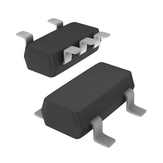
- Package: SOT753 (SC-70)
- Essence: Single-gate buffer/driver with tri-state output
- Packaging/Quantity: Tape and Reel, 3000 pieces per reel
Specifications
- Supply Voltage Range: 1.65V to 5.5V
- High-Level Input Voltage: 0.7 x VCC
- Low-Level Input Voltage: 0.3 x VCC
- High-Level Output Voltage: 0.9 x VCC
- Low-Level Output Voltage: 0.1 x VCC
- Maximum Output Current: ±32mA
- Propagation Delay: 4.2ns (typical)
- Operating Temperature Range: -40°C to +125°C
Detailed Pin Configuration
The 74LVC1G125GV-Q100 has a total of 5 pins: 1. GND (Ground) 2. A (Input) 3. OE (Output Enable) 4. Y (Output) 5. VCC (Power Supply)
Functional Features
- Tri-State Output: The OE pin allows the output to be disabled, putting it in a high-impedance state.
- Wide Supply Voltage Range: Can operate from 1.65V to 5.5V, making it compatible with various systems.
- High-Speed Operation: Provides fast signal propagation with a typical delay of 4.2ns.
- Low Power Consumption: Designed for low-voltage applications, minimizing power consumption.
Advantages and Disadvantages
Advantages: - Small package size enables space-saving designs. - Wide supply voltage range allows compatibility with different systems. - Tri-state output provides flexibility in controlling the output state.
Disadvantages: - Limited output current may not be suitable for high-current applications. - Propagation delay may affect timing-sensitive designs.
Working Principles
The 74LVC1G125GV-Q100 is a single-gate buffer/driver that amplifies and buffers digital signals. It operates by receiving an input signal at pin A, which is then amplified and transmitted to the output pin Y. The OE pin controls the output state, allowing it to be enabled or disabled. When disabled, the output enters a high-impedance state, effectively disconnecting it from the rest of the circuit.
Detailed Application Field Plans
The 74LVC1G125GV-Q100 is commonly used in various electronic devices and systems, including: - Mobile phones - Tablets - Portable media players - Wearable devices - IoT (Internet of Things) devices
It is particularly useful in applications where space is limited, and low-voltage operation is required. The tri-state output feature makes it suitable for bus-oriented systems, allowing multiple devices to share a common bus without interference.
Detailed and Complete Alternative Models
- SN74LVC1G125DBVR: SOT23-5 package, similar specifications
- MC74LVC1G125DTT1G: SOT-23-6 package, similar specifications
- TC7SZ125FU: SOT-353 package, similar specifications
These alternative models offer similar functionality and characteristics, providing options for different package preferences or availability.
In conclusion, the 74LVC1G125GV-Q100 is a versatile single-gate buffer/driver IC with a wide supply voltage range and tri-state output capability. Its small package size and low power consumption make it suitable for space-constrained and low-voltage applications. However, its limited output current and propagation delay should be considered for specific design requirements.
Sebutkan 10 pertanyaan dan jawaban umum terkait penerapan 74LVC1G125GV-Q100, dalam solusi teknis
Sure! Here are 10 common questions and answers related to the application of 74LVC1G125GV-Q100:
Q1: What is the 74LVC1G125GV-Q100? A1: The 74LVC1G125GV-Q100 is a single bus buffer gate with 3-state output, designed for low-voltage applications.
Q2: What is the operating voltage range of the 74LVC1G125GV-Q100? A2: The operating voltage range is from 1.65V to 5.5V.
Q3: What is the maximum output current of the 74LVC1G125GV-Q100? A3: The maximum output current is 32mA.
Q4: Can the 74LVC1G125GV-Q100 be used in high-speed applications? A4: Yes, it has a high-speed operation with a propagation delay of 3.8ns.
Q5: How many inputs does the 74LVC1G125GV-Q100 have? A5: It has one input.
Q6: Can the 74LVC1G125GV-Q100 be used as a level shifter? A6: Yes, it can be used as a level shifter to convert signals between different voltage levels.
Q7: Does the 74LVC1G125GV-Q100 have an enable pin? A7: No, it does not have an enable pin. The output is always active.
Q8: What is the package type of the 74LVC1G125GV-Q100? A8: It is available in a small SOT753 package.
Q9: Can the 74LVC1G125GV-Q100 drive capacitive loads? A9: Yes, it can drive capacitive loads up to 50pF.
Q10: Is the 74LVC1G125GV-Q100 suitable for automotive applications? A10: Yes, it is designed for automotive applications and meets the AEC-Q100 standard.
Please note that these answers are general and may vary depending on specific application requirements.