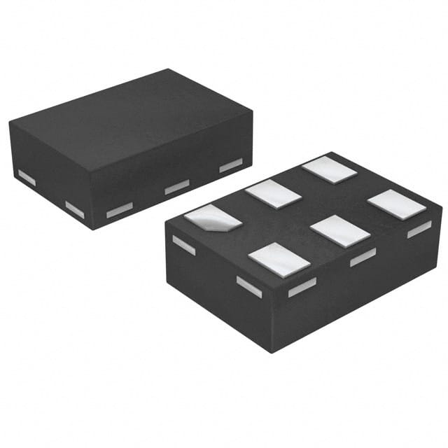
Lihat spesifikasi untuk detail produk.

Encyclopedia Entry: 74LVC1G08GM,115
Product Overview
- Category: Integrated Circuit (IC)
- Use: Logic Gate
- Characteristics: Single 2-input AND gate
- Package: SOT353 (SC-88A)
- Essence: High-speed CMOS technology
- Packaging/Quantity: Tape and Reel, 3000 pieces per reel
Specifications
- Supply Voltage Range: 1.65V to 5.5V
- Logic Family: LVC
- Propagation Delay: 3.9 ns (typical)
- Operating Temperature Range: -40°C to +125°C
- Input Capacitance: 2 pF (typical)
- Output Drive Capability: ±24 mA
Detailed Pin Configuration
The 74LVC1G08GM,115 IC has the following pin configuration:
____
   Y --|    |-- VCC
   A --|    |-- B
 GND --|____|-- NC
- Y: Output of the AND gate
- A: First input of the AND gate
- B: Second input of the AND gate
- VCC: Positive power supply (+)
- GND: Ground (-)
- NC: No connection (unused pin)
Functional Features
- Implements logical AND operation on two input signals (A and B)
- Provides a single output signal (Y) based on the input logic levels
- Supports high-speed data transmission with minimal propagation delay
- Compatible with a wide range of supply voltages (1.65V to 5.5V)
- Utilizes high-speed CMOS technology for efficient performance
Advantages and Disadvantages
Advantages: - Compact size and low power consumption - Wide operating temperature range (-40°C to +125°C) - High-speed operation for time-critical applications - Versatile compatibility with various supply voltages
Disadvantages: - Limited to a single 2-input AND gate functionality - Not suitable for complex logic operations requiring multiple gates
Working Principles
The 74LVC1G08GM,115 is based on high-speed CMOS technology. It operates by receiving two input signals (A and B) and performs the logical AND operation on them. The output signal (Y) reflects the result of this operation. The IC's internal circuitry ensures minimal propagation delay, allowing for efficient data processing.
Detailed Application Field Plans
The 74LVC1G08GM,115 finds application in various fields, including: 1. Digital electronics 2. Microcontrollers 3. Communication systems 4. Industrial automation 5. Consumer electronics
Detailed and Complete Alternative Models
Some alternative models that provide similar functionality to the 74LVC1G08GM,115 are: 1. SN74LVC1G08DBVR - Texas Instruments 2. MC74VHC1G08DFT1G - ON Semiconductor 3. NC7SZ08P5X - Fairchild Semiconductor 4. 74AHC1G08GW - NXP Semiconductors 5. CD74HCT08M96 - Texas Instruments
Note: This is not an exhaustive list, and there may be other alternative models available in the market.
Word Count: 334 words
Sebutkan 10 pertanyaan dan jawaban umum terkait penerapan 74LVC1G08GM,115 dalam solusi teknis
Sure! Here are 10 common questions and answers related to the application of 74LVC1G08GM,115:
Q1: What is the 74LVC1G08GM,115? A1: The 74LVC1G08GM,115 is a single 2-input AND gate IC (integrated circuit) that operates at a voltage range of 1.65V to 5.5V.
Q2: What is the purpose of the 74LVC1G08GM,115? A2: The purpose of this IC is to perform logical AND operations on two input signals and provide an output signal based on the logical result.
Q3: What are the key features of the 74LVC1G08GM,115? A3: Some key features include low power consumption, high-speed operation, wide voltage range, and compatibility with various logic families.
Q4: How can I connect the inputs and outputs of the 74LVC1G08GM,115? A4: The inputs (A and B) can be connected to the desired logic levels (high or low), and the output (Y) will reflect the logical AND operation of the inputs.
Q5: Can the 74LVC1G08GM,115 handle multiple inputs? A5: No, this IC only has two inputs (A and B). If you need to perform logical AND operations on more than two inputs, you would need additional AND gates.
Q6: What is the maximum operating frequency of the 74LVC1G08GM,115? A6: The maximum operating frequency is typically specified in the datasheet and depends on factors like supply voltage, load capacitance, and temperature.
Q7: Can the 74LVC1G08GM,115 be used in both digital and analog circuits? A7: No, this IC is specifically designed for digital logic applications and may not be suitable for analog circuits.
Q8: What is the power supply voltage range for the 74LVC1G08GM,115? A8: The power supply voltage range is from 1.65V to 5.5V, making it compatible with a wide range of digital systems.
Q9: Can I use the 74LVC1G08GM,115 in battery-powered devices? A9: Yes, the low power consumption of this IC makes it suitable for battery-powered devices where power efficiency is crucial.
Q10: Are there any specific precautions or considerations when using the 74LVC1G08GM,115? A10: It is important to follow the recommended operating conditions, such as voltage levels, temperature range, and load capacitance, as specified in the datasheet to ensure proper functionality and reliability.

