

Lihat spesifikasi untuk detail produk.
74LVC1G06GV,125
Basic Information Overview
- Category: Integrated Circuit (IC)
- Use: Logic Gate Inverter
- Characteristics: Low-voltage CMOS technology, high-speed operation, low power consumption
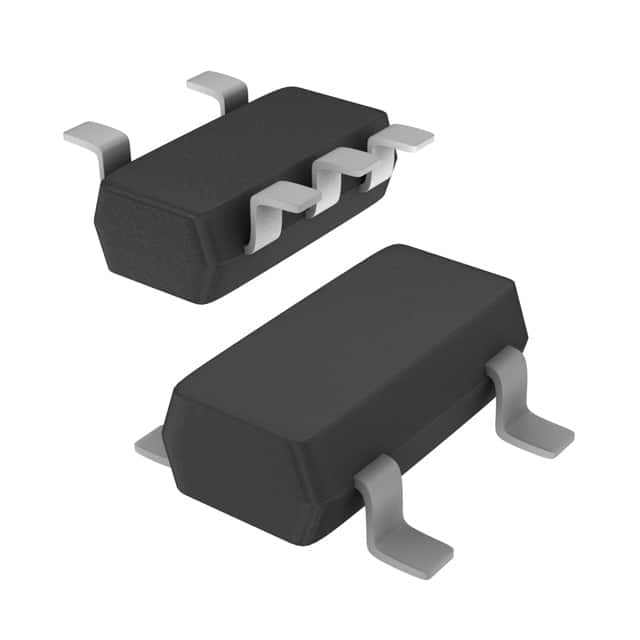
- Package: SOT753 (SC-70)
- Essence: Single gate inverter
- Packaging/Quantity: Tape and Reel, 3000 pieces per reel
Specifications
- Supply Voltage Range: 1.65V to 5.5V
- Input Voltage Range: -0.5V to VCC + 0.5V
- Output Voltage Range: -0.5V to VCC + 0.5V
- Maximum Operating Frequency: 160 MHz
- Propagation Delay: 4.3 ns (typical) at 3.3V supply voltage
Detailed Pin Configuration
The 74LVC1G06GV,125 has a total of 5 pins: 1. GND (Ground) 2. A (Input) 3. Y (Output) 4. NC (No Connection) 5. VCC (Power Supply)
Functional Features
- Single gate inverter with Schmitt-trigger input
- Converts logic levels from one voltage to another
- Provides signal inversion with hysteresis
- Suitable for interfacing different logic families
Advantages and Disadvantages
Advantages: - Low-voltage operation allows compatibility with various systems - High-speed operation enables quick signal processing - Low power consumption reduces energy requirements
Disadvantages: - Limited number of gates in a single package - Not suitable for high-power applications
Working Principles
The 74LVC1G06GV,125 is based on low-voltage CMOS technology. It utilizes a single gate inverter with a Schmitt-trigger input. When the input voltage crosses a certain threshold, the output switches state, providing signal inversion. The Schmitt-trigger input adds hysteresis, making the device less sensitive to noise and ensuring stable output transitions.
Detailed Application Field Plans
The 74LVC1G06GV,125 can be used in various applications, including: - Battery-powered devices - Portable electronics - Communication systems - Industrial automation - Automotive electronics
Detailed and Complete Alternative Models
Some alternative models that can be considered as replacements for the 74LVC1G06GV,125 are: - SN74LVC1G06DBVR (Texas Instruments) - MC74VHC1G14 (ON Semiconductor) - NC7SZ04P5X (Fairchild Semiconductor)
Note: These alternative models may have slightly different specifications and pin configurations. It is important to refer to their respective datasheets for detailed information.
This entry provides an overview of the 74LVC1G06GV,125 integrated circuit. It includes basic information, specifications, pin configuration, functional features, advantages and disadvantages, working principles, application field plans, and alternative models.
Sebutkan 10 pertanyaan dan jawaban umum terkait penerapan 74LVC1G06GV,125 dalam solusi teknis
Sure! Here are 10 common questions and answers related to the application of 74LVC1G06GV,125 in technical solutions:
Q1: What is the 74LVC1G06GV,125? A1: The 74LVC1G06GV,125 is a single inverter buffer with open-drain output, commonly used in digital logic circuits.
Q2: What is the voltage supply range for the 74LVC1G06GV,125? A2: The voltage supply range for the 74LVC1G06GV,125 is typically between 1.65V and 5.5V.
Q3: What is the maximum output current of the 74LVC1G06GV,125? A3: The maximum output current of the 74LVC1G06GV,125 is typically around 32mA.
Q4: Can the 74LVC1G06GV,125 be used as a level shifter? A4: Yes, the 74LVC1G06GV,125 can be used as a level shifter to convert signals between different voltage levels.
Q5: What is the propagation delay of the 74LVC1G06GV,125? A5: The propagation delay of the 74LVC1G06GV,125 is typically around 4.5ns.
Q6: Is the 74LVC1G06GV,125 compatible with both CMOS and TTL logic levels? A6: Yes, the 74LVC1G06GV,125 is compatible with both CMOS and TTL logic levels.
Q7: Can the 74LVC1G06GV,125 be used in high-speed applications? A7: Yes, the 74LVC1G06GV,125 is designed for high-speed operation and can be used in applications with fast switching requirements.
Q8: Does the 74LVC1G06GV,125 have built-in protection features? A8: Yes, the 74LVC1G06GV,125 has built-in protection against electrostatic discharge (ESD) and excessive power dissipation.
Q9: Can the 74LVC1G06GV,125 drive capacitive loads? A9: Yes, the 74LVC1G06GV,125 can drive capacitive loads up to a certain limit specified in the datasheet.
Q10: What package options are available for the 74LVC1G06GV,125? A10: The 74LVC1G06GV,125 is available in various package options, such as SOT23, SC-70, and XSON.