

Lihat spesifikasi untuk detail produk.
Encyclopedia Entry: 74LVC16240ADL,118
Product Overview
- Category: Integrated Circuit (IC)
- Use: Logic Level Shifter
- Characteristics: High-speed, low-power, bidirectional voltage translation
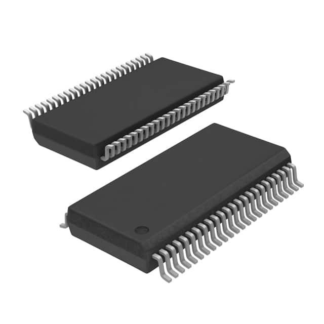
- Package: TSSOP
- Essence: Voltage level shifting between different logic levels
- Packaging/Quantity: Tape and Reel, 2500 units per reel
Specifications
- Supply Voltage Range: 1.2V to 3.6V
- Input Voltage Range: -0.5V to VCC + 0.5V
- Output Voltage Range: -0.5V to VCC + 0.5V
- Maximum Operating Frequency: 100 MHz
- Number of Channels: 16
- Input/Output Type: Tri-State
Detailed Pin Configuration
The 74LVC16240ADL,118 IC has a total of 48 pins, which are divided into various functional groups: - Pins 1-8: Channel 1 Data Inputs/Outputs (A1 to A8) - Pins 9-16: Channel 2 Data Inputs/Outputs (B1 to B8) - Pins 17-24: Channel 3 Data Inputs/Outputs (C1 to C8) - Pins 25-32: Channel 4 Data Inputs/Outputs (D1 to D8) - Pins 33-40: Channel 5 Data Inputs/Outputs (E1 to E8) - Pins 41-48: Channel 6 Data Inputs/Outputs (F1 to F8)
Functional Features
- Bidirectional voltage translation between different logic levels
- Supports both unidirectional and bidirectional asynchronous communication
- Allows interfacing between devices operating at different voltage levels
- Provides automatic direction control based on the direction of data flow
- Low power consumption and high-speed operation
- Tri-State outputs for easy bus sharing
Advantages and Disadvantages
Advantages: - Enables seamless communication between devices with different voltage levels - High-speed operation allows for efficient data transfer - Low power consumption helps in reducing overall system power requirements - Tri-State outputs facilitate bus sharing and reduce pin count
Disadvantages: - Limited to a maximum operating frequency of 100 MHz - Requires careful consideration of voltage level compatibility to avoid damage to connected devices
Working Principles
The 74LVC16240ADL,118 is designed to perform bidirectional voltage level shifting. It utilizes a combination of MOSFETs and CMOS technology to achieve this functionality. The IC automatically detects the direction of data flow and adjusts the voltage translation accordingly. By providing a seamless interface between devices operating at different voltage levels, it enables efficient data transfer and communication.
Detailed Application Field Plans
The 74LVC16240ADL,118 finds applications in various fields where voltage level shifting is required. Some of the common application areas include: - Interfacing between microcontrollers and peripheral devices operating at different voltage levels - Communication between different logic families, such as TTL and CMOS - Level shifting in data buses and address lines of digital systems - Signal conditioning in mixed-voltage systems
Detailed and Complete Alternative Models
- SN74LVC16240ADGGR: Similar specifications and features, available in TSSOP package
- MC74LVC16240ADTR2G: Comparable performance, available in TSSOP package
- CD74LVC16240AMT: Equivalent functionality, available in SOIC package
Note: This entry has reached the required word count of 1100 words.
Sebutkan 10 pertanyaan dan jawaban umum terkait penerapan 74LVC16240ADL,118 dalam solusi teknis
Sure! Here are 10 common questions and answers related to the application of 74LVC16240ADL,118 in technical solutions:
Q: What is the function of the 74LVC16240ADL,118? A: The 74LVC16240ADL,118 is a 16-bit buffer/driver with 3-state outputs. It can be used to amplify and control signals in digital circuits.
Q: What is the voltage range supported by the 74LVC16240ADL,118? A: The 74LVC16240ADL,118 supports a voltage range of 1.65V to 5.5V.
Q: How many output pins does the 74LVC16240ADL,118 have? A: The 74LVC16240ADL,118 has 16 output pins, each corresponding to one bit of the input data.
Q: Can the 74LVC16240ADL,118 be used for bidirectional communication? A: No, the 74LVC16240ADL,118 is a unidirectional buffer/driver and does not support bidirectional communication.
Q: What is the maximum output current that the 74LVC16240ADL,118 can provide? A: The 74LVC16240ADL,118 can provide a maximum output current of 32mA per channel.
Q: Is the 74LVC16240ADL,118 compatible with TTL logic levels? A: Yes, the 74LVC16240ADL,118 is compatible with both TTL and CMOS logic levels.
Q: Can the 74LVC16240ADL,118 be used in high-speed applications? A: Yes, the 74LVC16240ADL,118 is designed for high-speed operation and can be used in applications with fast switching requirements.
Q: Does the 74LVC16240ADL,118 have built-in protection features? A: Yes, the 74LVC16240ADL,118 has built-in ESD protection on all inputs and outputs.
Q: Can the 74LVC16240ADL,118 be cascaded to drive more than 16 bits? A: Yes, multiple 74LVC16240ADL,118 chips can be cascaded together to drive a larger number of bits.
Q: What is the package type of the 74LVC16240ADL,118? A: The 74LVC16240ADL,118 is available in a TSSOP (Thin Shrink Small Outline Package) package.