

Lihat spesifikasi untuk detail produk.
74LVC139BQ,115
Product Overview
- Category: Integrated Circuit (IC)
- Use: Decoder/Demultiplexer
- Characteristics: Low-voltage CMOS technology, high-speed operation, low power consumption
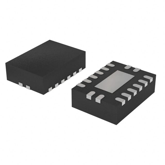
- Package: TSSOP-16
- Essence: Dual 2-to-4 line decoder/demultiplexer
- Packaging/Quantity: Tape and Reel, 2500 units per reel
Specifications
- Supply Voltage Range: 1.65V to 5.5V
- High-Level Input Voltage: 0.7 x VCC
- Low-Level Input Voltage: 0.3 x VCC
- High-Level Output Voltage: 0.9 x VCC
- Low-Level Output Voltage: 0.1 x VCC
- Maximum Operating Frequency: 100 MHz
- Propagation Delay: 6 ns (typical)
Detailed Pin Configuration
The 74LVC139BQ,115 has a total of 16 pins arranged as follows:
+---+--+---+
   A1 -|1  +--+ 16|- VCC
   A0 -|2         |- Y0
   E1 -|3         |- Y1
   E0 -|4         |- GND
   Y0 -|5         |- Y2
   Y1 -|6         |- Y3
   Y2 -|7         |- E1
   Y3 -|8         |- E0
GND/V -|9         |- A0
   Y4 -|10        |- A1
   Y5 -|11        |- nOE
   Y6 -|12        |- nOE
   Y7 -|13        |- Y6
   GND -|14        |- Y5
   Y8 -|15        |- Y4
       +---+--+---+
Functional Features
The 74LVC139BQ,115 is a dual 2-to-4 line decoder/demultiplexer IC. It takes two binary inputs (A1 and A0) and two enable inputs (E1 and E0) to generate four outputs (Y0 to Y3). The active-low enable inputs allow the user to select the desired output line. This IC operates at high speed while consuming low power due to its implementation using low-voltage CMOS technology.
Advantages and Disadvantages
Advantages: - High-speed operation - Low power consumption - Wide supply voltage range - Compact TSSOP-16 package
Disadvantages: - Limited number of output lines (4) - Lack of built-in protection features
Working Principles
The 74LVC139BQ,115 works based on the principles of digital logic. The binary inputs (A1 and A0) determine which output line is selected when the corresponding enable inputs (E1 and E0) are active. When an enable input is low (active), the selected output line will be low, while all other output lines remain high. The IC uses CMOS technology to achieve high-speed operation and low power consumption.
Detailed Application Field Plans
The 74LVC139BQ,115 can be used in various applications, including but not limited to: - Address decoding in microcontrollers and microprocessors - Data routing and selection in multiplexers - Memory address decoding - Signal demultiplexing
Detailed and Complete Alternative Models
Some alternative models that offer similar functionality to the 74LVC139BQ,115 include: - 74HC139: High-speed CMOS version with a wider supply voltage range - CD74HC139: High-speed CMOS version with Schmitt-trigger inputs - SN74LS139: Low-power Schottky TTL version
These alternative models can be considered based on specific requirements such as supply voltage range, speed, and power consumption.
Word count: 346 words
Sebutkan 10 pertanyaan dan jawaban umum terkait penerapan 74LVC139BQ,115 dalam solusi teknis
Sure! Here are 10 common questions and answers related to the application of 74LVC139BQ,115 in technical solutions:
1. What is the 74LVC139BQ,115? The 74LVC139BQ,115 is a dual 2-to-4 line decoder/demultiplexer IC that can be used in various digital logic applications.
2. What is the operating voltage range for the 74LVC139BQ,115? The operating voltage range for the 74LVC139BQ,115 is typically between 1.65V and 5.5V.
3. How many inputs does the 74LVC139BQ,115 have? The 74LVC139BQ,115 has two 2-inputs (A0, A1) for selecting the output lines.
4. How many output lines does the 74LVC139BQ,115 have? The 74LVC139BQ,115 has four output lines (Y0, Y1, Y2, Y3).
5. What is the maximum output current of the 74LVC139BQ,115? The maximum output current of the 74LVC139BQ,115 is typically 32mA.
6. Can the 74LVC139BQ,115 be used as a demultiplexer? Yes, the 74LVC139BQ,115 can be used as a demultiplexer by connecting the appropriate input lines.
7. What is the propagation delay of the 74LVC139BQ,115? The propagation delay of the 74LVC139BQ,115 is typically around 4.5ns.
8. Is the 74LVC139BQ,115 compatible with TTL logic levels? Yes, the 74LVC139BQ,115 is compatible with both TTL and CMOS logic levels.
9. Can the 74LVC139BQ,115 be cascaded to increase the number of output lines? Yes, multiple 74LVC139BQ,115 ICs can be cascaded together to increase the number of output lines.
10. What are some common applications of the 74LVC139BQ,115? Some common applications of the 74LVC139BQ,115 include address decoding, data routing, memory selection, and general-purpose digital logic circuits.
Please note that the answers provided here are general and may vary depending on specific datasheet specifications and application requirements.