

Lihat spesifikasi untuk detail produk.
74LV1T125GXH
Product Overview
- Category: Logic Gates
- Use: Buffer/Driver
- Characteristics: Single gate, non-inverting, tri-state output
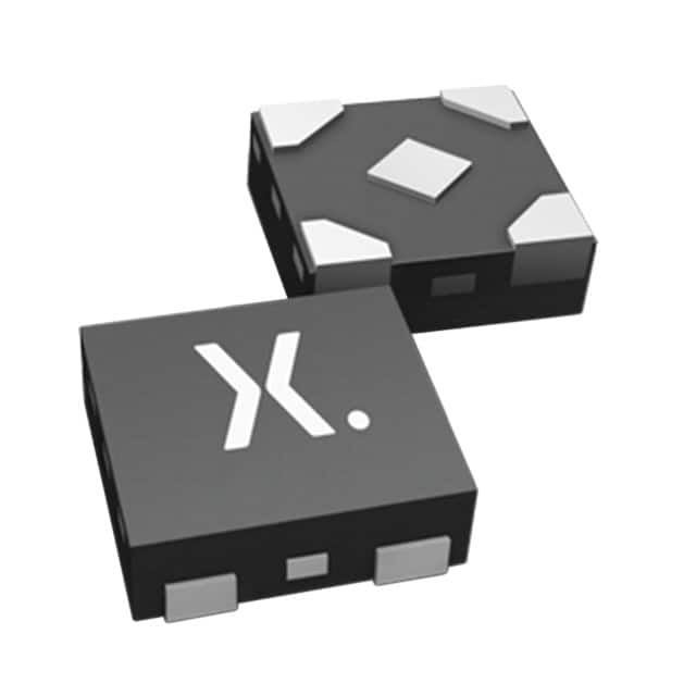
- Package: SOT753 (XSON6)
- Essence: High-speed CMOS technology
- Packaging/Quantity: Tape and Reel, 3000 pieces per reel
Specifications
- Supply Voltage Range: 1.65V to 5.5V
- Input Voltage Range: 0V to VCC
- Output Voltage Range: 0V to VCC
- Maximum Operating Frequency: 400MHz
- Propagation Delay: 3.8ns (typical)
- Output Drive Capability: ±24mA
Detailed Pin Configuration
The 74LV1T125GXH has a total of 6 pins:
- GND (Ground)
- A (Input)
- OE (Output Enable)
- Y (Output)
- VCC (Power Supply)
- B (Input)
Functional Features
- Non-inverting buffer/driver with tri-state output
- Allows bidirectional data flow
- High-speed operation suitable for various applications
- Low power consumption
- Schmitt-trigger input for noise immunity
Advantages and Disadvantages
Advantages: - Wide supply voltage range allows compatibility with different systems - Tri-state output enables bus sharing and reduces contention issues - High-speed operation makes it suitable for time-critical applications - Low power consumption helps in energy-efficient designs
Disadvantages: - Limited output drive capability may not be suitable for driving heavy loads - Only a single gate is available in the package, limiting flexibility in complex designs
Working Principles
The 74LV1T125GXH is a non-inverting buffer/driver that amplifies and buffers digital signals. It features a tri-state output, which allows the output to be disconnected from the bus when not in use. This feature enables multiple devices to share the same bus without causing contention issues.
The device operates on high-speed CMOS technology, providing fast switching times and low power consumption. The Schmitt-trigger input ensures noise immunity by providing hysteresis and reducing the effects of signal noise.
Detailed Application Field Plans
The 74LV1T125GXH is commonly used in various applications, including:
- Communication systems: It can be used as a buffer/driver for data transmission between different modules or devices.
- Industrial automation: The tri-state output enables bus sharing in control systems, allowing multiple devices to communicate efficiently.
- Consumer electronics: It can be utilized in audio/video equipment, computer peripherals, and other digital devices that require signal buffering.
Detailed and Complete Alternative Models
- 74LVC1T45GW: Single gate, non-inverting, tri-state buffer with higher output drive capability.
- 74LV1T126GXH: Single gate, non-inverting, tri-state buffer with additional input/output options.
- 74LVC1G07GW: Single gate, open-drain buffer with Schmitt-trigger input.
These alternative models offer similar functionality but may have different specifications or package options to suit specific design requirements.
In conclusion, the 74LV1T125GXH is a versatile logic gate that serves as a buffer/driver with a tri-state output. Its high-speed operation, low power consumption, and compatibility with various supply voltages make it suitable for a wide range of applications in communication systems, industrial automation, and consumer electronics.
Sebutkan 10 pertanyaan dan jawaban umum terkait penerapan 74LV1T125GXH dalam solusi teknis
Sure! Here are 10 common questions and answers related to the application of 74LV1T125GXH in technical solutions:
Q1: What is the 74LV1T125GXH? A1: The 74LV1T125GXH is a single bus buffer gate with three-state output, designed for low-voltage (1.65V to 5.5V) applications.
Q2: What is the purpose of the 74LV1T125GXH? A2: The 74LV1T125GXH is used to buffer and level shift digital signals in various electronic circuits and systems.
Q3: What is the maximum operating frequency of the 74LV1T125GXH? A3: The maximum operating frequency of the 74LV1T125GXH is typically around 400 MHz.
Q4: What is the input voltage range of the 74LV1T125GXH? A4: The 74LV1T125GXH has an input voltage range from ground (0V) to VCC (supply voltage).
Q5: Can the 74LV1T125GXH be used in both CMOS and TTL logic systems? A5: Yes, the 74LV1T125GXH is compatible with both CMOS and TTL logic levels.
Q6: How many channels does the 74LV1T125GXH have? A6: The 74LV1T125GXH has one channel, which means it can buffer a single digital signal.
Q7: What is the output drive capability of the 74LV1T125GXH? A7: The 74LV1T125GXH has a typical output drive capability of ±24 mA.
Q8: Can the 74LV1T125GXH be used in bidirectional applications? A8: No, the 74LV1T125GXH is a unidirectional buffer and cannot be used for bidirectional communication.
Q9: What is the power supply voltage range for the 74LV1T125GXH? A9: The 74LV1T125GXH operates within a power supply voltage range of 1.65V to 5.5V.
Q10: Is the 74LV1T125GXH available in different package options? A10: Yes, the 74LV1T125GXH is available in various package options, such as SOT23, XSON, and TSSOP.
Please note that these answers are general and may vary depending on the specific datasheet and manufacturer's specifications for the 74LV1T125GXH.