

Lihat spesifikasi untuk detail produk.
74HCT3G07GD,125
Basic Information Overview
- Category: Integrated Circuit (IC)
- Use: Logic Buffer/Driver
- Characteristics: High-speed, low-power, non-inverting buffer/driver
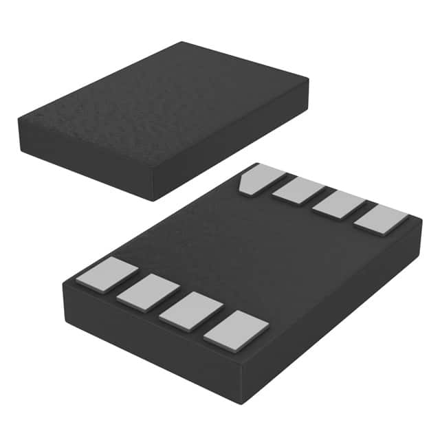
- Package: SOT353 (SC-88A)
- Essence: Hex buffer/driver with open-drain outputs
- Packaging/Quantity: Tape and Reel, 3000 pieces per reel
Specifications
- Supply Voltage Range: 2.0V to 6.0V
- Input Voltage Range: 0V to VCC
- Output Voltage Range: 0V to VCC
- Maximum Operating Frequency: 80 MHz
- Output Current: ±4 mA
- Propagation Delay: 7 ns (typical)
Detailed Pin Configuration
The 74HCT3G07GD,125 IC has a total of six pins: 1. GND (Ground) 2. A1 (Input A1) 3. Y1 (Output Y1) 4. A2 (Input A2) 5. Y2 (Output Y2) 6. VCC (Supply Voltage)
Functional Features
- Hex non-inverting buffer/driver with open-drain outputs
- Provides high-speed signal amplification and level shifting
- Allows bidirectional communication between different voltage domains
- Supports voltage translation between TTL and CMOS logic levels
- Enables wired-OR connections for multiple devices
Advantages and Disadvantages
Advantages: - High-speed operation allows for fast data transmission - Low power consumption helps in reducing overall system energy usage - Open-drain outputs provide flexibility in interfacing with other devices - Wide supply voltage range enables compatibility with various systems
Disadvantages: - Limited output current may restrict driving capability for certain applications - Propagation delay can affect timing-sensitive operations - SOT353 package may require careful handling during assembly
Working Principles
The 74HCT3G07GD,125 is a hex buffer/driver IC that amplifies and shifts logic level signals. It features open-drain outputs, which means the outputs can either pull the signal low or remain in a high-impedance state. This allows for wired-OR connections, where multiple devices can share a common bus line.
The IC operates by receiving input signals on the A1 and A2 pins. These signals are then amplified and inverted internally before being driven to the corresponding Y1 and Y2 output pins. The VCC pin provides the necessary supply voltage, while the GND pin serves as the ground reference.
Detailed Application Field Plans
The 74HCT3G07GD,125 IC finds applications in various fields, including: 1. Communication Systems: Used for level shifting and signal buffering in data communication interfaces. 2. Industrial Automation: Enables interfacing between different logic voltage levels in control systems. 3. Automotive Electronics: Facilitates bidirectional communication between microcontrollers and sensors/actuators. 4. Consumer Electronics: Provides voltage translation between different logic families in audio/video equipment.
Detailed and Complete Alternative Models
Some alternative models to the 74HCT3G07GD,125 IC include: - SN74LVC3G07: Similar hex buffer/driver with open-drain outputs from Texas Instruments. - MC74VHC1G07: Single non-inverting buffer/driver with open-drain output from ON Semiconductor. - CD4050B: Hex non-inverting buffer/driver with high-voltage capability from Texas Instruments.
Note: The above alternatives have similar functionalities but may differ in specifications and package options.
This entry provides an overview of the 74HCT3G07GD,125 IC, including its basic information, specifications, pin configuration, functional features, advantages and disadvantages, working principles, application field plans, and alternative models.
Sebutkan 10 pertanyaan dan jawaban umum terkait penerapan 74HCT3G07GD,125 dalam solusi teknis
Sure! Here are 10 common questions and answers related to the application of 74HCT3G07GD,125 in technical solutions:
Q: What is the function of the 74HCT3G07GD,125? A: The 74HCT3G07GD,125 is a hex buffer with open-drain outputs. It can be used for level shifting, signal buffering, and driving high-current loads.
Q: What is the voltage range supported by the 74HCT3G07GD,125? A: The 74HCT3G07GD,125 supports a voltage range of 2V to 5.5V.
Q: How many buffers are there in the 74HCT3G07GD,125? A: The 74HCT3G07GD,125 has six buffers in a single package.
Q: Can the 74HCT3G07GD,125 be used for bidirectional communication? A: No, the 74HCT3G07GD,125 is unidirectional and can only be used for one-way signal transmission.
Q: What is the maximum output current of the 74HCT3G07GD,125? A: The 74HCT3G07GD,125 can provide a maximum output current of 25mA per channel.
Q: Is the 74HCT3G07GD,125 compatible with TTL logic levels? A: Yes, the 74HCT3G07GD,125 is compatible with both CMOS and TTL logic levels.
Q: Can the 74HCT3G07GD,125 be used in automotive applications? A: Yes, the 74HCT3G07GD,125 is AEC-Q100 qualified and suitable for automotive applications.
Q: What is the operating temperature range of the 74HCT3G07GD,125? A: The 74HCT3G07GD,125 can operate in a temperature range of -40°C to +125°C.
Q: Does the 74HCT3G07GD,125 have built-in protection features? A: Yes, the 74HCT3G07GD,125 has built-in ESD protection on all inputs and outputs.
Q: Can the 74HCT3G07GD,125 be used in battery-powered applications? A: Yes, the 74HCT3G07GD,125 has low power consumption and can be used in battery-powered devices.
Please note that the answers provided here are general and may vary depending on specific application requirements.