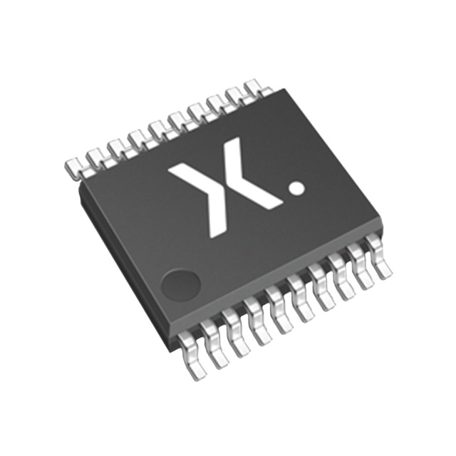
Lihat spesifikasi untuk detail produk.

74HC241PW,112
Product Overview
- Category: Integrated Circuit (IC)
- Use: Logic Level Shifter
- Characteristics: High-speed, CMOS technology
- Package: TSSOP (Thin Shrink Small Outline Package)
- Essence: Buffer/Line Driver
- Packaging/Quantity: Tape and Reel, 2500 units per reel
Specifications
- Supply Voltage Range: 2.0V to 6.0V
- Input Voltage Range: 0V to VCC
- Output Voltage Range: 0V to VCC
- High-Level Input Voltage: 0.7 x VCC to VCC
- Low-Level Input Voltage: 0V to 0.3 x VCC
- High-Level Output Voltage: 0.9 x VCC to VCC
- Low-Level Output Voltage: 0V to 0.1 x VCC
- Maximum Operating Frequency: 80 MHz
- Number of Inputs: 8
- Number of Outputs: 8
Detailed Pin Configuration
The 74HC241PW,112 has a total of 20 pins arranged as follows:
+---+--+---+
   A1 -|1  +--+ 20|- VCC
   A2 -|2         |- B1
   A3 -|3         |- B2
   A4 -|4         |- B3
   A5 -|5         |- B4
   A6 -|6         |- B5
   A7 -|7         |- B6
   A8 -|8         |- B7
 GND -|9         |- B8
  OE -|10        |- GND
  Y1 -|11        |- A8
  Y2 -|12        |- A7
  Y3 -|13        |- A6
  Y4 -|14        |- A5
  Y5 -|15        |- A4
  Y6 -|16        |- A3
  Y7 -|17        |- A2
  Y8 -|18        |- A1
  GND-|19        |- OE
       +----------+
Functional Features
The 74HC241PW,112 is a high-speed CMOS logic level shifter. It is designed to convert signals between different voltage levels, making it suitable for interfacing between devices operating at different voltage levels. The device features 8 inputs and 8 outputs, allowing bidirectional signal conversion.
Advantages and Disadvantages
Advantages: - High-speed operation - Wide supply voltage range - Bidirectional signal conversion - Compact TSSOP package
Disadvantages: - Limited number of inputs and outputs - Not suitable for high-power applications
Working Principles
The 74HC241PW,112 operates based on CMOS technology. It utilizes a combination of MOSFETs (Metal-Oxide-Semiconductor Field-Effect Transistors) to achieve the desired logic level shifting functionality. When an input signal is received, the device amplifies and shifts the voltage level to match the output requirements.
Detailed Application Field Plans
The 74HC241PW,112 finds applications in various fields where voltage level shifting is required. Some common application areas include:
- Microcontroller interfacing: The IC can be used to interface microcontrollers operating at different voltage levels.
- Communication systems: It can be employed in communication systems to convert signals between different voltage domains.
- Sensor networks: The device enables seamless integration of sensors operating at different voltage levels.
- Industrial automation: It can be utilized in industrial automation systems to interface different control modules.
Detailed and Complete Alternative Models
- 74HCT241PW,112: Similar to the 74HC241PW,112 but operates at a lower supply voltage range of 4.5V to 5.5V.
- SN74LVC1G241DBVR: A single-channel logic level shifter with similar functionality but in a different package (SOT-23).
These alternative models provide similar voltage level shifting capabilities and can be considered as substitutes for the 74HC241PW,112 depending on specific requirements.
Word count: 515 words
Sebutkan 10 pertanyaan dan jawaban umum terkait penerapan 74HC241PW,112 dalam solusi teknis
Sure! Here are 10 common questions and answers related to the application of 74HC241PW,112 in technical solutions:
Q: What is the 74HC241PW,112? A: The 74HC241PW,112 is a 3-state octal buffer/line driver with input latches.
Q: What is the purpose of the 74HC241PW,112? A: It is used to provide buffering and signal amplification for digital signals in various electronic circuits.
Q: What voltage levels does the 74HC241PW,112 support? A: It supports a wide range of voltage levels, typically from 2V to 6V.
Q: How many inputs and outputs does the 74HC241PW,112 have? A: It has 8 inputs and 8 outputs.
Q: Can the 74HC241PW,112 be used as a bidirectional buffer? A: No, it is a unidirectional buffer and cannot be used for bidirectional communication.
Q: What is the maximum current that the 74HC241PW,112 can source or sink? A: The maximum current per output is typically around 6mA.
Q: Can the 74HC241PW,112 handle high-speed signals? A: Yes, it is designed to operate at high speeds, making it suitable for applications requiring fast signal propagation.
Q: Does the 74HC241PW,112 have built-in protection features? A: Yes, it has built-in diode clamps to protect against electrostatic discharge (ESD) and other voltage spikes.
Q: Can the 74HC241PW,112 be cascaded to increase the number of outputs? A: Yes, multiple 74HC241PW,112 chips can be cascaded to increase the number of outputs in a system.
Q: What are some common applications of the 74HC241PW,112? A: It is commonly used in bus driving, memory address decoding, and general-purpose digital logic circuits.
Please note that the answers provided here are general and may vary depending on specific datasheet specifications and application requirements.

