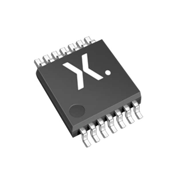
Lihat spesifikasi untuk detail produk.

74HC11PW,112
Product Overview
- Category: Integrated Circuit (IC)
- Use: Logic Gate
- Characteristics: Triple 3-input AND gate
- Package: TSSOP-14
- Essence: High-speed CMOS logic gate
- Packaging/Quantity: Tape and Reel, 2500 units per reel
Specifications
- Supply Voltage Range: 2.0V to 6.0V
- Input Voltage Range: -0.5V to VCC + 0.5V
- Output Voltage Range: -0.5V to VCC + 0.5V
- Operating Temperature Range: -40°C to +125°C
- Propagation Delay: 10 ns (typical)
- Maximum Quiescent Current: 1 µA at 5.5V
- Maximum Input Current: ±1 µA at 5.5V
- Maximum Output Current: ±25 mA at 5.5V
Detailed Pin Configuration
The 74HC11PW,112 has a TSSOP-14 package with the following pin configuration:
__    __
   A1 | 1    14 | VCC
   B1 | 2    13 | C1
   A2 | 3    12 | B3
   B2 | 4    11 | C3
   A3 | 5    10 | C2
   B3 | 6     9 | B2
  GND | 7     8 | A2
       ‾‾    ‾‾
Functional Features
- Triple 3-input AND gate with Schmitt-trigger inputs
- High noise immunity due to Schmitt-trigger inputs
- Wide operating voltage range
- Low power consumption
- High-speed operation
Advantages and Disadvantages
Advantages: - Schmitt-trigger inputs provide noise immunity - Wide operating voltage range allows for versatile applications - Low power consumption makes it suitable for battery-powered devices - High-speed operation enables efficient signal processing
Disadvantages: - Limited to AND gate functionality only - TSSOP package may require specialized handling during assembly
Working Principles
The 74HC11PW,112 is a logic gate that performs the AND operation on three input signals. It utilizes Schmitt-trigger inputs, which provide hysteresis and improve noise immunity. When all three inputs are high (logic level 1), the output of the gate becomes high. Otherwise, the output remains low (logic level 0). The gate operates within a wide voltage range and consumes minimal power.
Detailed Application Field Plans
The 74HC11PW,112 can be used in various applications, including:
- Digital systems: It can be employed in digital circuits for logical operations, such as data processing, control units, and arithmetic functions.
- Communication systems: The gate can be utilized in communication devices for signal conditioning, filtering, and modulation/demodulation processes.
- Industrial automation: It finds application in industrial control systems, robotics, and process control units for logical decision-making and signal manipulation.
- Automotive electronics: The gate can be integrated into automotive systems for controlling sensors, actuators, and safety features.
- Consumer electronics: It can be used in devices like smartphones, tablets, and gaming consoles for various logical operations and signal processing tasks.
Detailed and Complete Alternative Models
Some alternative models to the 74HC11PW,112 include:
- SN74LS11N: Triple 3-input AND gate with standard TTL logic levels.
- CD4073B: Triple 3-input AND gate with CMOS logic levels.
- MC74HC11A: Triple 3-input AND gate with advanced high-speed CMOS technology.
These alternative models offer similar functionality but may differ in terms of voltage range, power consumption, and package type.
Word count: 470 words
Sebutkan 10 pertanyaan dan jawaban umum terkait penerapan 74HC11PW,112 dalam solusi teknis
Sure! Here are 10 common questions and answers related to the application of 74HC11PW,112 in technical solutions:
Q: What is the 74HC11PW,112? A: The 74HC11PW,112 is a triple 3-input AND gate integrated circuit (IC) that can be used in various digital logic applications.
Q: What is the operating voltage range for the 74HC11PW,112? A: The operating voltage range for the 74HC11PW,112 is typically between 2V and 6V.
Q: Can the 74HC11PW,112 be used in both TTL and CMOS logic systems? A: Yes, the 74HC11PW,112 is compatible with both TTL and CMOS logic systems.
Q: What is the maximum output current of the 74HC11PW,112? A: The maximum output current of the 74HC11PW,112 is typically around 5.2mA.
Q: How many inputs does the 74HC11PW,112 have? A: The 74HC11PW,112 has three inputs per gate, making it a triple 3-input AND gate.
Q: Can the 74HC11PW,112 be used for level shifting applications? A: Yes, the 74HC11PW,112 can be used for level shifting applications as it supports both high-level and low-level input voltages.
Q: What is the propagation delay of the 74HC11PW,112? A: The propagation delay of the 74HC11PW,112 is typically around 9ns.
Q: Is the 74HC11PW,112 available in different package types? A: Yes, the 74HC11PW,112 is available in various package types, such as TSSOP and SOIC.
Q: Can the 74HC11PW,112 be used for signal conditioning applications? A: Yes, the 74HC11PW,112 can be used for signal conditioning applications where logical AND operations are required.
Q: Are there any recommended application circuits available for the 74HC11PW,112? A: Yes, the datasheet of the 74HC11PW,112 provides recommended application circuits that can help in understanding its usage in different scenarios.
Please note that these answers are general and may vary depending on specific datasheets and application requirements.

