Lihat spesifikasi untuk detail produk.

Encyclopedia Entry: 74AXP1G125GNH
Product Information Overview
- Category: Integrated Circuit (IC)
- Use: Logic Buffer/Driver
- Characteristics: High-speed, low-power, single gate buffer/driver
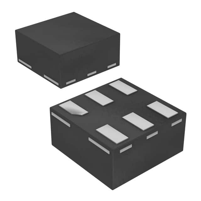
- Package: SOT-753 (Thin SOT-23) package
- Essence: Provides buffering and driving capabilities for digital signals
- Packaging/Quantity: Available in reels of 3000 units
Specifications
- Supply Voltage: 1.65V to 5.5V
- Input Voltage Range (VI): GND to VCC
- Output Voltage Range (VO): GND to VCC
- Operating Temperature Range: -40°C to +85°C
- Propagation Delay (tpd): 2.3ns (typical) at 3.3V supply voltage
- Output Drive Capability: ±24mA at 3.3V supply voltage
Detailed Pin Configuration
The 74AXP1G125GNH IC has the following pin configuration:
____
   Y ---|    |
   A ---|    |
   B ---|    |
  GND --|    |
  VCC --|____|
Functional Features
- Single gate buffer/driver with tri-state output
- Compatible with various logic families (including TTL, CMOS, and LVCMOS)
- Provides signal buffering and driving capabilities
- Supports bidirectional data flow
- Low power consumption
- High-speed operation
Advantages
- Small form factor package allows for space-efficient designs
- Wide operating voltage range enables compatibility with different systems
- Tri-state output allows for bus sharing and multi-master configurations
- High-speed operation enhances overall system performance
- Low power consumption helps conserve energy
Disadvantages
- Limited output drive capability may not be suitable for high-current applications
- Single gate design restricts the number of signals that can be buffered/driven simultaneously
Working Principles
The 74AXP1G125GNH is a logic buffer/driver IC that operates by receiving digital input signals (A) and providing buffered output signals (Y). The device is powered by a supply voltage (VCC) within the specified range. When enabled, the input signal is amplified and transmitted to the output pin. The tri-state output feature allows the device to enter a high-impedance state, effectively disconnecting the output from the bus when not in use.
Detailed Application Field Plans
The 74AXP1G125GNH finds applications in various fields, including:
- Microcontrollers and embedded systems
- Communication systems
- Industrial automation
- Consumer electronics
- Automotive electronics
Detailed and Complete Alternative Models
Some alternative models that offer similar functionality to the 74AXP1G125GNH are:
- SN74LVC1G125DBVR - Texas Instruments
- MC74VHC1GT125DF1G - ON Semiconductor
- NC7SZ125P5X - Fairchild Semiconductor
- TC7SZ125FU - Toshiba Semiconductor
These alternatives provide comparable buffering and driving capabilities, but designers should consider specific requirements and compatibility with existing systems before selecting an alternative model.
Word count: 346 words
Sebutkan 10 pertanyaan dan jawaban umum terkait penerapan 74AXP1G125GNH dalam solusi teknis
Sure! Here are 10 common questions and answers related to the application of 74AXP1G125GNH in technical solutions:
Q1: What is the 74AXP1G125GNH? A1: The 74AXP1G125GNH is a single bus buffer gate with 3-state output, designed for voltage level translation applications.
Q2: What is the operating voltage range of 74AXP1G125GNH? A2: The operating voltage range of 74AXP1G125GNH is from 1.65V to 5.5V.
Q3: What is the maximum output current of 74AXP1G125GNH? A3: The maximum output current of 74AXP1G125GNH is typically 32mA.
Q4: Can 74AXP1G125GNH be used for bidirectional level shifting? A4: No, 74AXP1G125GNH is a unidirectional buffer gate and cannot be used for bidirectional level shifting.
Q5: What is the propagation delay of 74AXP1G125GNH? A5: The propagation delay of 74AXP1G125GNH is typically around 2.5ns.
Q6: Can 74AXP1G125GNH be used in high-speed applications? A6: Yes, 74AXP1G125GNH is suitable for high-speed applications due to its low propagation delay.
Q7: How many inputs does 74AXP1G125GNH have? A7: 74AXP1G125GNH has one input pin.
Q8: How many outputs does 74AXP1G125GNH have? A8: 74AXP1G125GNH has one output pin.
Q9: Can 74AXP1G125GNH be used in automotive applications? A9: Yes, 74AXP1G125GNH is AEC-Q100 qualified and can be used in automotive applications.
Q10: What is the package type of 74AXP1G125GNH? A10: 74AXP1G125GNH is available in a small SOT-353 package.

