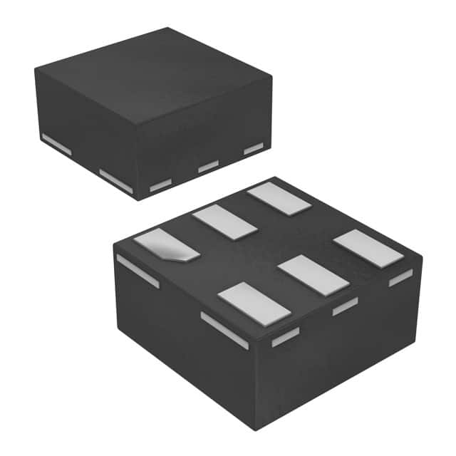
Lihat spesifikasi untuk detail produk.

Encyclopedia Entry: 74AUP1G34GF,132
Product Overview
Category
The 74AUP1G34GF,132 belongs to the category of integrated circuits (ICs) and specifically falls under the logic gates subcategory.
Use
This product is primarily used for signal amplification and processing in digital electronic circuits. It serves as a single buffer gate with an output that can drive high capacitive loads.
Characteristics
- Low power consumption
- High-speed operation
- Wide operating voltage range
- Small package size
- RoHS compliant
Package
The 74AUP1G34GF,132 is available in a small form factor package, such as SOT353 or XSON6.
Essence
The essence of this product lies in its ability to provide reliable signal buffering and amplification in various digital circuit applications.
Packaging/Quantity
The 74AUP1G34GF,132 is typically packaged in reels or tubes, containing a quantity of 3000 units per reel/tube.
Specifications
- Supply Voltage Range: 0.8V to 3.6V
- Input Voltage Range: 0V to VCC
- Output Voltage Range: 0V to VCC
- Operating Temperature Range: -40°C to +85°C
- Propagation Delay: <5ns
- Maximum Quiescent Current: 10μA
Detailed Pin Configuration
The 74AUP1G34GF,132 has the following pin configuration:
____
   A --|    |-- VCC
   Y --|    |-- GND
       ----
Functional Features
- Single buffer gate with one input (A) and one output (Y)
- Provides non-inverting signal amplification
- Can drive high capacitive loads
- Compatible with various logic families
Advantages and Disadvantages
Advantages
- Low power consumption makes it suitable for battery-powered devices
- High-speed operation enables efficient signal processing
- Wide operating voltage range allows compatibility with different systems
- Small package size saves board space
Disadvantages
- Limited functionality as a single buffer gate
- May not be suitable for applications requiring complex logic operations
Working Principles
The 74AUP1G34GF,132 operates based on the principles of CMOS (Complementary Metal-Oxide-Semiconductor) technology. It utilizes MOSFET transistors to amplify and buffer digital signals. The input signal is amplified and inverted by the internal circuitry, providing an amplified output signal.
Detailed Application Field Plans
The 74AUP1G34GF,132 finds application in various digital electronic circuits, including but not limited to: - Microcontrollers - Data communication systems - Signal conditioning circuits - Sensor interfaces - Battery-powered devices
Detailed and Complete Alternative Models
Some alternative models that offer similar functionality to the 74AUP1G34GF,132 include: - SN74LVC1G34DBVR - MC74VHC1G34DTT1G - TC7SZ34FU
These alternatives can be considered based on specific requirements and availability.
In conclusion, the 74AUP1G34GF,132 is a versatile integrated circuit that serves as a single buffer gate, providing reliable signal amplification and buffering in digital electronic circuits. Its low power consumption, high-speed operation, and wide operating voltage range make it suitable for various applications. However, its limited functionality as a single gate may require alternative models for more complex logic operations.
Sebutkan 10 pertanyaan dan jawaban umum terkait penerapan 74AUP1G34GF,132 dalam solusi teknis
Sure! Here are 10 common questions and answers related to the application of 74AUP1G34GF,132 in technical solutions:
Q1: What is the function of the 74AUP1G34GF,132? A1: The 74AUP1G34GF,132 is a single buffer gate with open-drain output. It is commonly used for level shifting and signal buffering in various electronic circuits.
Q2: What is the voltage supply range for the 74AUP1G34GF,132? A2: The 74AUP1G34GF,132 operates within a voltage supply range of 0.8V to 3.6V.
Q3: What is the maximum output current of the 74AUP1G34GF,132? A3: The maximum output current of the 74AUP1G34GF,132 is typically around 32mA.
Q4: Can the 74AUP1G34GF,132 be used for level shifting between different voltage domains? A4: Yes, the 74AUP1G34GF,132 can be used for level shifting between voltage domains due to its wide operating voltage range.
Q5: Is the 74AUP1G34GF,132 suitable for high-speed applications? A5: Yes, the 74AUP1G34GF,132 is designed for high-speed operation and can handle data rates up to several hundred megahertz.
Q6: Does the 74AUP1G34GF,132 have built-in protection features? A6: Yes, the 74AUP1G34GF,132 has built-in ESD (electrostatic discharge) protection on all inputs and outputs.
Q7: Can the 74AUP1G34GF,132 be used in both digital and analog circuits? A7: The 74AUP1G34GF,132 is primarily designed for digital applications, but it can also be used in certain low-frequency analog circuits.
Q8: What is the typical propagation delay of the 74AUP1G34GF,132? A8: The typical propagation delay of the 74AUP1G34GF,132 is around 2.5 nanoseconds.
Q9: Can the 74AUP1G34GF,132 drive capacitive loads? A9: Yes, the 74AUP1G34GF,132 can drive small capacitive loads typically found in most digital circuits.
Q10: Is the 74AUP1G34GF,132 available in different package options? A10: Yes, the 74AUP1G34GF,132 is available in various package options, such as SOT23, XSON, and DFN, to suit different application requirements.
Please note that the answers provided here are general and may vary depending on specific datasheet specifications and application conditions.

