Lihat spesifikasi untuk detail produk.

Encyclopedia Entry: 74AUP1G125GW-Q100H
Product Overview
Category
The 74AUP1G125GW-Q100H belongs to the category of integrated circuits (ICs), specifically a single bus buffer gate.
Use
This product is commonly used in electronic devices and systems for signal buffering and level shifting purposes. It ensures smooth and reliable data transmission between different components within a circuit.
Characteristics
- Low power consumption: The 74AUP1G125GW-Q100H is designed to operate with minimal power requirements, making it suitable for battery-powered devices.
- High-speed operation: This IC offers fast switching times, enabling efficient data transfer in time-critical applications.
- Wide voltage range: It supports a wide supply voltage range, allowing compatibility with various systems.
- Small package size: The 74AUP1G125GW-Q100H is available in a compact package, making it ideal for space-constrained designs.
- RoHS compliant: This product adheres to the Restriction of Hazardous Substances directive, ensuring environmental friendliness.
Package and Quantity
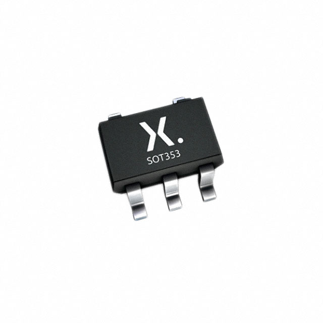
The 74AUP1G125GW-Q100H is typically packaged in a surface-mount SOT353 package. Each package contains a single IC.
Specifications
- Supply Voltage Range: 0.8V to 3.6V
- Input Voltage Range: -0.5V to VCC + 0.5V
- Output Voltage Range: -0.5V to VCC + 0.5V
- Operating Temperature Range: -40°C to 125°C
- Maximum Quiescent Current: 10μA
- Maximum Propagation Delay: 2.5ns
Detailed Pin Configuration
The 74AUP1G125GW-Q100H features a total of five pins:
- GND (Ground): Connected to the ground reference of the circuit.
- VCC (Power Supply): Connected to the positive supply voltage.
- A (Input): Receives the input signal to be buffered or level-shifted.
- Y (Output): Provides the buffered or level-shifted output signal.
- OE (Output Enable): Controls the output state, enabling or disabling the buffer.
Functional Features
The main functional features of the 74AUP1G125GW-Q100H include:
- Buffering: The IC amplifies and buffers the input signal, ensuring its integrity during transmission.
- Level Shifting: It adjusts the voltage levels of the input signal to match the requirements of the connected components.
- Output Enable Control: The OE pin allows for easy control of the output state, enabling or disabling the buffer as needed.
Advantages and Disadvantages
Advantages
- Low power consumption makes it suitable for battery-powered devices.
- High-speed operation enables efficient data transfer in time-critical applications.
- Wide voltage range ensures compatibility with various systems.
- Small package size facilitates space-constrained designs.
- RoHS compliance ensures environmental friendliness.
Disadvantages
- Limited number of input/output pins restricts the versatility of the IC.
- May not be suitable for applications requiring complex logic functions.
Working Principles
The 74AUP1G125GW-Q100H operates based on CMOS (Complementary Metal-Oxide-Semiconductor) technology. It utilizes a combination of NMOS (N-channel Metal-Oxide-Semiconductor) and PMOS (P-channel Metal-Oxide-Semiconductor) transistors to achieve buffering and level shifting functionalities. When an input signal is received, the IC amplifies and buffers it, adjusting the voltage levels if necessary, and provides the output signal accordingly.
Detailed Application Field Plans
The 74AUP1G125GW-Q100H finds applications in various electronic systems, including but not limited to:
- Mobile Devices: Used for signal buffering and level shifting in smartphones, tablets, and wearables.
- Automotive Electronics: Employed in automotive control units, infotainment systems, and sensor interfaces.
- Industrial Automation: Utilized in PLCs (Programmable Logic Controllers), motor control circuits, and sensor networks.
- Consumer Electronics: Integrated into audio/video equipment, gaming consoles, and home automation systems.
Detailed Alternative Models
For similar functionality and performance, alternative models to the 74AUP1G125GW-Q100H include:
- SN74LVC1G125DBVR
- MC74VHC1GT125DF1G
- TC7SZ125FU
These alternatives offer comparable features and can be considered based on specific design requirements.
Word count: 550 words
Sebutkan 10 pertanyaan dan jawaban umum terkait penerapan 74AUP1G125GW-Q100H dalam solusi teknis
Sure! Here are 10 common questions and answers related to the application of 74AUP1G125GW-Q100H in technical solutions:
Q1: What is the 74AUP1G125GW-Q100H? A1: The 74AUP1G125GW-Q100H is a single bus buffer gate with 3-state output, designed for low-power applications.
Q2: What is the operating voltage range of the 74AUP1G125GW-Q100H? A2: The operating voltage range is from 0.8V to 3.6V.
Q3: What is the maximum output current of the 74AUP1G125GW-Q100H? A3: The maximum output current is 32mA.
Q4: Can the 74AUP1G125GW-Q100H be used in automotive applications? A4: Yes, the 74AUP1G125GW-Q100H is qualified for automotive applications and meets the AEC-Q100 standard.
Q5: What is the typical propagation delay of the 74AUP1G125GW-Q100H? A5: The typical propagation delay is 2.5ns.
Q6: Can the 74AUP1G125GW-Q100H be used as a level shifter? A6: Yes, the 74AUP1G125GW-Q100H can be used as a level shifter due to its wide operating voltage range.
Q7: Does the 74AUP1G125GW-Q100H have internal pull-up or pull-down resistors? A7: No, the 74AUP1G125GW-Q100H does not have internal pull-up or pull-down resistors.
Q8: Is the 74AUP1G125GW-Q100H compatible with other logic families? A8: Yes, the 74AUP1G125GW-Q100H is compatible with a wide range of logic families, including TTL and CMOS.
Q9: Can the 74AUP1G125GW-Q100H drive capacitive loads? A9: Yes, the 74AUP1G125GW-Q100H can drive capacitive loads up to 50pF.
Q10: What is the package type of the 74AUP1G125GW-Q100H? A10: The 74AUP1G125GW-Q100H is available in a small SOT753 package.

