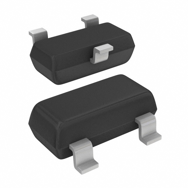
Lihat spesifikasi untuk detail produk.

Encyclopedia Entry: 74ALVCH16952DGG,11
Product Information Overview
- Category: Integrated Circuit (IC)
- Use: Logic Level Translator
- Characteristics: High-speed, low-power, bidirectional voltage translation
- Package: DGG package (Dual-Gate Gullwing), 56 pins
- Essence: This IC is designed to provide bidirectional voltage level translation between two independent voltage domains. It can be used in various applications where different voltage levels need to communicate with each other.
- Packaging/Quantity: The 74ALVCH16952DGG,11 is typically sold in reels or tubes containing multiple units.
Specifications
- Supply Voltage Range: 1.2V to 3.6V
- Input Voltage Range (A/B Ports): -0.5V to VCC + 0.5V
- Output Voltage Range (A/B Ports): -0.5V to VCC + 0.5V
- Operating Temperature Range: -40°C to +85°C
- Propagation Delay: < 4.5 ns (typical)
- Output Drive Capability: ±24 mA
Detailed Pin Configuration
The 74ALVCH16952DGG,11 has a total of 56 pins, which are assigned specific functions. Here is a brief overview of the pin configuration:
- Pin 1-28: A-side I/O ports (A1-A28)
- Pin 29: GND (Ground)
- Pin 30-57: B-side I/O ports (B1-B28)
- Pin 58: VCC (Power Supply)
For a detailed pin diagram and function description, please refer to the datasheet provided by the manufacturer.
Functional Features
- Bidirectional voltage level translation between two independent voltage domains.
- Supports voltage translation from 1.2V to 3.6V, making it compatible with a wide range of devices.
- High-speed operation with low propagation delay ensures efficient data transfer.
- Low-power consumption makes it suitable for battery-powered applications.
- Robust output drive capability allows for reliable signal transmission.
Advantages and Disadvantages
Advantages: - Wide supply voltage range enables compatibility with various systems. - Fast propagation delay ensures quick data transfer. - Low power consumption helps conserve energy in portable devices. - Robust output drive capability ensures reliable signal transmission.
Disadvantages: - Limited number of I/O ports (28 per side) may not be sufficient for complex applications requiring a higher number of connections. - The DGG package may require additional care during soldering due to its specific pin arrangement.
Working Principles
The 74ALVCH16952DGG,11 operates based on the principles of voltage level translation. It utilizes internal circuitry to convert signals from one voltage domain to another bidirectionally. The IC employs a combination of MOSFETs and other components to achieve efficient and accurate voltage translation.
Detailed Application Field Plans
The 74ALVCH16952DGG,11 can be used in various applications that require voltage level translation between different voltage domains. Some potential application fields include:
- Microcontroller interfacing with different voltage peripherals.
- Communication between devices operating at different voltage levels.
- Signal conversion in mixed-voltage systems.
- Interface bridging in multi-voltage environments.
Detailed and Complete Alternative Models
While the 74ALVCH16952DGG,11 offers specific features and characteristics, there are alternative models available in the market that serve similar purposes. Some alternative models worth considering include:
- SN74LVC8T245PW: 8-bit bidirectional voltage level translator with a wide supply voltage range.
- TXB0108PWR: 8-bit bidirectional voltage-level translator with automatic direction sensing.
- PCA9306DCUR: Dual bidirectional I2C-bus and SMBus voltage-level translator.
These alternative models provide similar functionality and can be evaluated based on specific application requirements.
Note: The above content provides an overview of the requested information. Additional details, such as pin diagrams and complete alternative models, can be found in the datasheet provided by the manufacturer.
Sebutkan 10 pertanyaan dan jawaban umum terkait penerapan 74ALVCH16952DGG,11 dalam solusi teknis
Sure! Here are 10 common questions and answers related to the application of 74ALVCH16952DGG,11 in technical solutions:
Q: What is the function of the 74ALVCH16952DGG,11? A: The 74ALVCH16952DGG,11 is a 16-bit universal bus transceiver with 3-state outputs. It can be used for bidirectional data transfer between two buses.
Q: What is the operating voltage range of the 74ALVCH16952DGG,11? A: The 74ALVCH16952DGG,11 operates within a voltage range of 1.65V to 3.6V.
Q: How many channels does the 74ALVCH16952DGG,11 have? A: The 74ALVCH16952DGG,11 has 16 channels, allowing it to handle 16 bits of data simultaneously.
Q: Can the 74ALVCH16952DGG,11 be used in both input and output modes? A: Yes, the 74ALVCH16952DGG,11 can be used as both an input and output device, making it versatile for various applications.
Q: What is the maximum data transfer rate supported by the 74ALVCH16952DGG,11? A: The 74ALVCH16952DGG,11 supports high-speed data transfer rates up to 400 Mbps.
Q: Does the 74ALVCH16952DGG,11 have built-in ESD protection? A: Yes, the 74ALVCH16952DGG,11 is designed with built-in ESD protection, ensuring robustness against electrostatic discharge.
Q: Can the 74ALVCH16952DGG,11 be used in automotive applications? A: Yes, the 74ALVCH16952DGG,11 is suitable for automotive applications as it meets the necessary standards and requirements.
Q: What is the power supply current consumption of the 74ALVCH16952DGG,11? A: The power supply current consumption of the 74ALVCH16952DGG,11 varies depending on the operating conditions but typically ranges from a few milliamperes to tens of milliamperes.
Q: Does the 74ALVCH16952DGG,11 support hot-plugging of devices? A: Yes, the 74ALVCH16952DGG,11 supports hot-plugging, allowing devices to be connected or disconnected while the system is powered on.
Q: Are there any specific layout considerations when using the 74ALVCH16952DGG,11? A: Yes, it is recommended to follow the manufacturer's guidelines for proper PCB layout, including signal integrity, decoupling capacitors, and minimizing noise coupling between traces.
Please note that the answers provided here are general and may vary based on specific datasheet information and application requirements.

