

Lihat spesifikasi untuk detail produk.
74AHC3G14DC-Q100H
Basic Information Overview
- Category: Integrated Circuit (IC)
- Use: Logic Gate
- Characteristics: Triple Inverter Schmitt Trigger
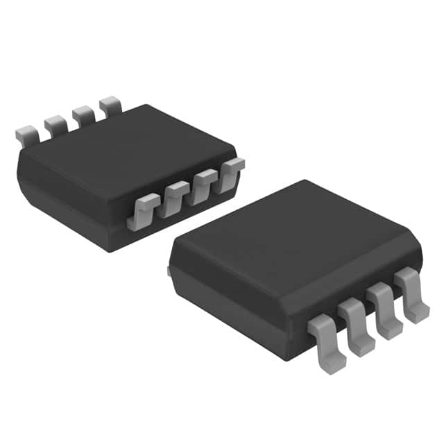
- Package: SOT-23
- Essence: High-Speed CMOS Technology
- Packaging/Quantity: Tape and Reel, 3000 pieces per reel
Specifications
- Supply Voltage Range: 2.0V to 5.5V
- Input Voltage Range: 0V to VCC
- Output Voltage Range: 0V to VCC
- Operating Temperature Range: -40°C to +125°C
- Propagation Delay: 4.5 ns (typical) at 5V
- Output Drive Capability: ±24 mA at 3.3V
Detailed Pin Configuration
The 74AHC3G14DC-Q100H has a total of six pins:
- Pin 1: Input A
- Pin 2: Input B
- Pin 3: Output C
- Pin 4: Ground (GND)
- Pin 5: Power Supply (VCC)
- Pin 6: Not Connected (NC)
Functional Features
- Triple inverter Schmitt trigger with hysteresis
- High noise immunity
- Wide operating voltage range
- Low power consumption
- Fast switching speed
- Balanced propagation delays
Advantages and Disadvantages
Advantages: - Provides reliable signal conditioning and level shifting - Suitable for high-speed digital applications - Offers improved noise immunity compared to standard inverters
Disadvantages: - Limited output drive capability - Requires external pull-up or pull-down resistors for proper operation
Working Principles
The 74AHC3G14DC-Q100H is based on high-speed CMOS technology. It consists of three inverters with Schmitt trigger inputs. The Schmitt trigger provides hysteresis, allowing the circuit to have different voltage thresholds for rising and falling input signals. This feature improves noise immunity and reduces the likelihood of false triggering.
The IC operates within a wide supply voltage range of 2.0V to 5.5V, making it compatible with various digital systems. It consumes low power and exhibits fast switching speeds, making it suitable for high-speed applications.
Detailed Application Field Plans
The 74AHC3G14DC-Q100H is commonly used in the following application fields:
- Digital signal conditioning
- Level shifting
- Oscillators and clock generation circuits
- Signal amplification and buffering
- Sensor interfaces
- Communication systems
- Industrial automation
Detailed and Complete Alternative Models
- SN74LVC3G14-Q1: Triple Inverter Schmitt Trigger, SOT-23 package
- MC74VHC1G14: Single Inverter Schmitt Trigger, SOT-23 package
- CD40106B: Hex Schmitt Trigger, SOIC package
- 74HC14: Hex Inverter Schmitt Trigger, DIP package
- TC7SZ14FU: Single Inverter Schmitt Trigger, SOT-353 package
These alternative models offer similar functionality and can be used as replacements for the 74AHC3G14DC-Q100H in various applications.
In conclusion, the 74AHC3G14DC-Q100H is a triple inverter Schmitt trigger IC that provides reliable signal conditioning and level shifting capabilities. Its high-speed CMOS technology, wide operating voltage range, and low power consumption make it suitable for a variety of digital applications. However, it has limited output drive capability and requires external resistors for proper operation. It finds applications in digital signal conditioning, level shifting, and various other fields such as communication systems and industrial automation. Alternative models with similar functionality are available for substitution if needed.
Sebutkan 10 pertanyaan dan jawaban umum terkait penerapan 74AHC3G14DC-Q100H dalam solusi teknis
Sure! Here are 10 common questions and answers related to the application of 74AHC3G14DC-Q100H in technical solutions:
Q: What is the 74AHC3G14DC-Q100H? A: The 74AHC3G14DC-Q100H is a triple Schmitt-trigger inverter IC, which can be used for signal conditioning and level shifting applications.
Q: What is the operating voltage range of the 74AHC3G14DC-Q100H? A: The operating voltage range of the 74AHC3G14DC-Q100H is from 2.0V to 5.5V.
Q: What is the maximum output current of the 74AHC3G14DC-Q100H? A: The maximum output current of the 74AHC3G14DC-Q100H is typically 8mA.
Q: Can the 74AHC3G14DC-Q100H be used for level shifting between different voltage domains? A: Yes, the 74AHC3G14DC-Q100H can be used for level shifting between different voltage domains due to its wide operating voltage range.
Q: What is the propagation delay of the 74AHC3G14DC-Q100H? A: The propagation delay of the 74AHC3G14DC-Q100H is typically 6 ns.
Q: Is the 74AHC3G14DC-Q100H suitable for high-speed applications? A: Yes, the 74AHC3G14DC-Q100H is designed for high-speed operation and can be used in applications with fast switching requirements.
Q: Does the 74AHC3G14DC-Q100H have built-in ESD protection? A: Yes, the 74AHC3G14DC-Q100H has built-in ESD protection, making it more robust against electrostatic discharge events.
Q: Can the 74AHC3G14DC-Q100H be used in automotive applications? A: Yes, the 74AHC3G14DC-Q100H is qualified for automotive applications and meets the AEC-Q100 standard.
Q: What is the package type of the 74AHC3G14DC-Q100H? A: The 74AHC3G14DC-Q100H is available in a small SOT353 package.
Q: Are there any application notes or reference designs available for the 74AHC3G14DC-Q100H? A: Yes, the manufacturer provides application notes and reference designs that can help in implementing the 74AHC3G14DC-Q100H in various technical solutions.
Please note that the answers provided here are general and may vary depending on the specific datasheet and manufacturer's documentation for the 74AHC3G14DC-Q100H.