

Lihat spesifikasi untuk detail produk.
74AHC1G79GV-Q100H
Basic Information Overview
- Category: Integrated Circuit (IC)
- Use: Logic Gate
- Characteristics: High-speed, low-power, single positive-edge triggered D-type flip-flop
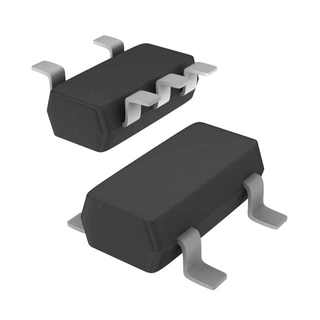
- Package: SOT353 (SC-88A)
- Essence: Single D-type flip-flop with clear input
- Packaging/Quantity: Tape and Reel, 3000 pieces per reel
Specifications
- Supply Voltage Range: 2.0V to 5.5V
- High-Level Input Voltage: 0.7 x VCC
- Low-Level Input Voltage: 0.3 x VCC
- High-Level Output Current: -8 mA
- Low-Level Output Current: 8 mA
- Operating Temperature Range: -40°C to +125°C
Detailed Pin Configuration
The 74AHC1G79GV-Q100H has a total of 6 pins: 1. Pin 1: Data Input (D) 2. Pin 2: Clear Input (CLR) 3. Pin 3: Clock Input (CLK) 4. Pin 4: Output (Q) 5. Pin 5: Ground (GND) 6. Pin 6: Power Supply (VCC)
Functional Features
- Single positive-edge triggered D-type flip-flop
- Provides a buffered output
- Clear input for asynchronous reset
- High-speed operation
- Low power consumption
- Schmitt-trigger action on all inputs
Advantages and Disadvantages
Advantages: - High-speed operation allows for efficient data processing - Low power consumption helps in reducing energy usage - Schmitt-trigger action ensures noise immunity and reliable operation
Disadvantages: - Limited number of flip-flops in a single package - Not suitable for applications requiring multiple flip-flops
Working Principles
The 74AHC1G79GV-Q100H is a single positive-edge triggered D-type flip-flop. It stores and transfers data based on the clock input signal. The clear input allows for asynchronous reset, clearing the stored data. The flip-flop operates at high speed and consumes low power, making it suitable for various logic applications.
Detailed Application Field Plans
The 74AHC1G79GV-Q100H can be used in a wide range of applications, including: - Digital communication systems - Computer peripherals - Industrial control systems - Consumer electronics - Automotive electronics
Detailed and Complete Alternative Models
Some alternative models to the 74AHC1G79GV-Q100H are: - SN74LVC1G79DBVR - MC74VHC1G79DTT1G - TC7SZ79FU
These models offer similar functionality and can be used as alternatives depending on specific requirements.
Word count: 238 words
Sebutkan 10 pertanyaan dan jawaban umum terkait penerapan 74AHC1G79GV-Q100H dalam solusi teknis
Sure! Here are 10 common questions and answers related to the application of 74AHC1G79GV-Q100H in technical solutions:
Q1: What is the 74AHC1G79GV-Q100H? A1: The 74AHC1G79GV-Q100H is a single positive-edge triggered D-type flip-flop with reset. It is a versatile integrated circuit commonly used in digital logic applications.
Q2: What is the operating voltage range of the 74AHC1G79GV-Q100H? A2: The 74AHC1G79GV-Q100H operates within a voltage range of 2.0V to 5.5V, making it suitable for various low-power applications.
Q3: How many flip-flops are there in the 74AHC1G79GV-Q100H? A3: The 74AHC1G79GV-Q100H consists of a single flip-flop, which means it can store and manipulate one bit of data.
Q4: Can the 74AHC1G79GV-Q100H be used for edge-triggered or level-triggered operations? A4: No, the 74AHC1G79GV-Q100H is specifically designed for positive-edge triggered operations only.
Q5: What is the maximum clock frequency supported by the 74AHC1G79GV-Q100H? A5: The 74AHC1G79GV-Q100H can operate at a maximum clock frequency of 200 MHz, allowing for high-speed data processing.
Q6: Does the 74AHC1G79GV-Q100H have an asynchronous reset feature? A6: Yes, the 74AHC1G79GV-Q100H has an asynchronous reset input (RESET) that can be used to reset the flip-flop to a known state.
Q7: What is the typical propagation delay of the 74AHC1G79GV-Q100H? A7: The typical propagation delay of the 74AHC1G79GV-Q100H is around 5 ns, which indicates the time taken for the output to respond to a change in input.
Q8: Can the 74AHC1G79GV-Q100H drive external loads directly? A8: Yes, the 74AHC1G79GV-Q100H has a high output drive capability, allowing it to drive standard TTL or CMOS logic levels without the need for additional buffering.
Q9: Is the 74AHC1G79GV-Q100H suitable for automotive applications? A9: Yes, the 74AHC1G79GV-Q100H is specifically designed for automotive applications and meets the AEC-Q100 automotive qualification standards.
Q10: Are there any specific precautions to consider when using the 74AHC1G79GV-Q100H? A10: It is important to ensure proper decoupling capacitors are used near the power supply pins to minimize noise and voltage fluctuations. Additionally, care should be taken to avoid exceeding the maximum operating conditions specified in the datasheet.
Please note that these answers are general and may vary depending on the specific application and requirements.