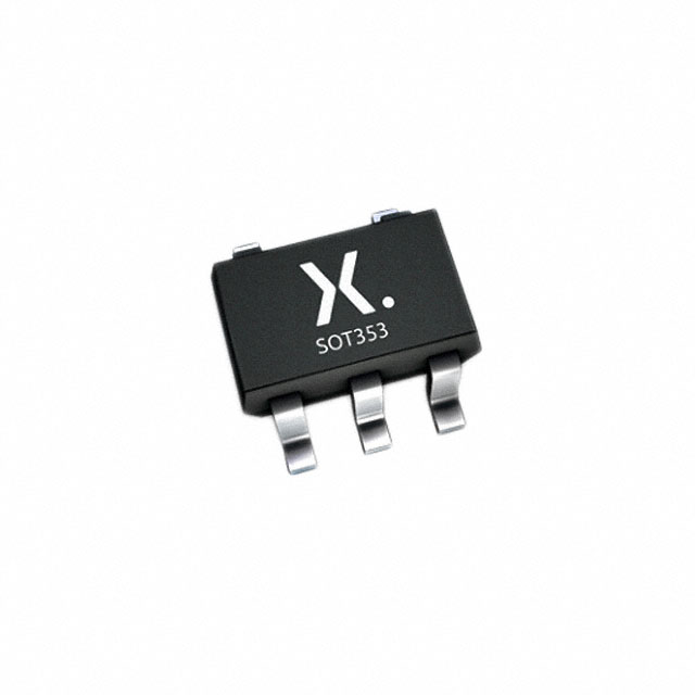
Lihat spesifikasi untuk detail produk.

Encyclopedia Entry: 74AHC1G126GW-Q100H
Product Overview
- Category: Integrated Circuit (IC)
- Use: Logic Gate Buffer/Driver
- Characteristics: High-speed, low-power consumption
- Package: SOT753 (SC-70)
- Essence: Single gate buffer with tri-state output
- Packaging/Quantity: Tape and Reel, 3000 units per reel
Specifications
The 74AHC1G126GW-Q100H is a logic gate buffer/driver integrated circuit. It operates at high speed while consuming low power. The IC is packaged in the SOT753 (SC-70) package, which is compact and suitable for space-constrained applications. Each reel of the product contains 3000 units.
Detailed Pin Configuration
The 74AHC1G126GW-Q100H has a total of 5 pins: 1. Pin 1: Input (I) 2. Pin 2: Output (O) 3. Pin 3: Enable (E) 4. Pin 4: Ground (GND) 5. Pin 5: Power Supply (VCC)
Functional Features
- Single gate buffer with tri-state output
- Provides buffering and driving capabilities for digital signals
- Tri-state output allows for high impedance state when not enabled
- Compatible with various logic families
- Supports wide operating voltage range
Advantages and Disadvantages
Advantages: - High-speed operation enables efficient signal processing - Low power consumption reduces energy usage - Compact package size allows for space-saving designs - Tri-state output provides flexibility in signal routing
Disadvantages: - Limited number of gates per IC (single gate only) - May require additional components for complex logic functions
Working Principles
The 74AHC1G126GW-Q100H operates as a buffer/driver for digital signals. It receives an input signal at Pin 1 and amplifies it to a higher current level at the output (Pin 2). The enable pin (Pin 3) controls the tri-state output, allowing the IC to enter a high impedance state when not enabled. This feature is useful in multi-driver systems where multiple devices share a common bus.
Detailed Application Field Plans
The 74AHC1G126GW-Q100H is commonly used in various applications, including: - Microcontrollers and microprocessors - Communication systems - Industrial automation - Automotive electronics - Consumer electronics
In microcontroller-based systems, this IC can be used to interface between the microcontroller and other peripheral devices, providing signal buffering and driving capabilities. In communication systems, it helps in signal conditioning and level shifting. In automotive electronics, it can be utilized for sensor interfacing and control signal generation. Its compact size makes it suitable for space-constrained designs in consumer electronics.
Detailed and Complete Alternative Models
Some alternative models that offer similar functionality to the 74AHC1G126GW-Q100H include: - SN74LVC1G126DBVR - MC74VHC1G126DF1G - TC7SZ126AFK(TE85L,F)
These alternatives may have slight variations in specifications or package types but serve the same purpose of buffering and driving digital signals.
Word count: 383 words
Sebutkan 10 pertanyaan dan jawaban umum terkait penerapan 74AHC1G126GW-Q100H dalam solusi teknis
Sure! Here are 10 common questions and answers related to the application of 74AHC1G126GW-Q100H in technical solutions:
Q1: What is the 74AHC1G126GW-Q100H? A1: The 74AHC1G126GW-Q100H is a single bus buffer gate with 3-state output, designed for use in automotive applications.
Q2: What is the operating voltage range of the 74AHC1G126GW-Q100H? A2: The operating voltage range is from 2.0V to 5.5V.
Q3: What is the maximum output current of the 74AHC1G126GW-Q100H? A3: The maximum output current is 8mA.
Q4: Can the 74AHC1G126GW-Q100H be used in high-speed applications? A4: Yes, it can be used in high-speed applications as it has a propagation delay of only 6ns.
Q5: Is the 74AHC1G126GW-Q100H compatible with other logic families? A5: Yes, it is compatible with both CMOS and TTL logic families.
Q6: Does the 74AHC1G126GW-Q100H have built-in ESD protection? A6: Yes, it has built-in ESD protection up to 2kV.
Q7: Can the 74AHC1G126GW-Q100H drive capacitive loads? A7: Yes, it can drive capacitive loads up to 50pF.
Q8: What is the temperature range for the 74AHC1G126GW-Q100H? A8: The temperature range is from -40°C to +125°C.
Q9: Can the 74AHC1G126GW-Q100H be used in automotive applications? A9: Yes, it is specifically designed for automotive applications and meets the AEC-Q100 standard.
Q10: What is the package type of the 74AHC1G126GW-Q100H? A10: It is available in a small SOT353 package.
Please note that these answers are based on general information about the 74AHC1G126GW-Q100H. For specific details and application requirements, it is recommended to refer to the datasheet or consult the manufacturer.

