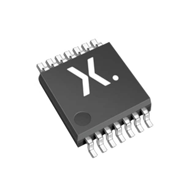
Lihat spesifikasi untuk detail produk.

Encyclopedia Entry: 74ABT08PW,118
Product Overview
Category
The 74ABT08PW,118 belongs to the category of integrated circuits (ICs). Specifically, it falls under the category of logic gates.
Use
This product is primarily used for logical operations in digital electronic circuits. It serves as a quad 2-input AND gate, allowing for the combination of multiple input signals to produce an output signal based on the AND logic function.
Characteristics
- Quad 2-input AND gate
- High-speed operation
- Low power consumption
- Wide operating voltage range
- Compatible with TTL and CMOS logic families
Package
The 74ABT08PW,118 is available in a small-outline package (SO) with 14 pins. This package type ensures easy integration into circuit boards and provides mechanical stability.
Essence
The essence of the 74ABT08PW,118 lies in its ability to perform logical AND operations on two input signals, providing a single output signal based on the result.
Packaging/Quantity
This product is typically packaged in reels or tubes, containing a specific quantity of ICs per package. The exact packaging and quantity may vary depending on the manufacturer and supplier.
Specifications
- Supply Voltage Range: 4.5V to 5.5V
- Input Voltage Range: 0V to VCC
- Output Voltage Range: 0V to VCC
- Operating Temperature Range: -40°C to +85°C
- Propagation Delay Time: 3.5ns (max)
- Input Capacitance: 3pF (typ)
- Output Current: ±24mA
Detailed Pin Configuration
The 74ABT08PW,118 has a total of 14 pins, each serving a specific purpose. The pin configuration is as follows:
- Input A1
- Input B1
- Output Y1
- Ground (GND)
- Input A2
- Input B2
- Output Y2
- VCC (Supply Voltage)
- Input A3
- Input B3
- Output Y3
- Input A4
- Input B4
- Output Y4
Functional Features
- High-speed operation allows for efficient processing of input signals.
- Low power consumption ensures energy efficiency in electronic circuits.
- Wide operating voltage range enables compatibility with various systems.
- Compatibility with TTL and CMOS logic families provides versatility in circuit design.
Advantages and Disadvantages
Advantages
- Fast propagation delay time enhances overall system performance.
- Low power consumption reduces energy requirements.
- Wide operating voltage range increases flexibility in circuit integration.
- Compatibility with multiple logic families simplifies circuit design.
Disadvantages
- Limited number of inputs and outputs restricts the complexity of logical operations.
- Sensitivity to electrostatic discharge (ESD) requires proper handling during installation and usage.
Working Principles
The 74ABT08PW,118 operates based on the AND logic function. It takes two input signals and produces an output signal that is high only when both inputs are high. If any of the inputs are low, the output will be low. This behavior follows the truth table for the AND gate:
| Input A | Input B | Output Y | |---------|---------|----------| | 0 | 0 | 0 | | 0 | 1 | 0 | | 1 | 0 | 0 | | 1 | 1 | 1 |
Detailed Application Field Plans
The 74ABT08PW,118 finds applications in various fields where logical operations are required. Some of the common application areas include:
- Digital electronics
- Microprocessor systems
- Communication systems
- Control systems
- Data processing units
Detailed and Complete Alternative Models
There are several alternative models available that serve similar functions to the 74ABT08PW,118. Some notable alternatives include:
- 74LS08: A TTL logic gate with similar characteristics and pin configuration.
- CD4081: A CMOS quad 2-input AND gate offering comparable performance.
- SN74HC08: A high-speed CMOS quad 2-input AND gate with improved power consumption.
These alternative models can be considered based on specific requirements and compatibility with existing circuit designs.
In conclusion, the 74ABT08PW,118 is a quad 2-input AND gate integrated circuit that offers high-speed operation, low power consumption, and wide operating voltage range. It finds applications in digital electronics, microprocessor systems, communication systems, control systems, and data processing units. While it has limitations in terms of input/output count
Sebutkan 10 pertanyaan dan jawaban umum terkait penerapan 74ABT08PW,118 dalam solusi teknis
Sure! Here are 10 common questions and answers related to the application of 74ABT08PW,118 in technical solutions:
Q: What is the function of the 74ABT08PW,118? A: The 74ABT08PW,118 is a quad 2-input AND gate integrated circuit that performs logical AND operations on two input signals.
Q: What is the operating voltage range for the 74ABT08PW,118? A: The operating voltage range for the 74ABT08PW,118 is typically between 4.5V and 5.5V.
Q: Can the 74ABT08PW,118 be used with both TTL and CMOS logic levels? A: Yes, the 74ABT08PW,118 is compatible with both TTL and CMOS logic levels, making it versatile for various applications.
Q: What is the maximum output current of the 74ABT08PW,118? A: The maximum output current of the 74ABT08PW,118 is typically around 32mA.
Q: How many inputs does the 74ABT08PW,118 have? A: The 74ABT08PW,118 has four inputs, allowing you to perform AND operations on multiple input signals.
Q: What is the propagation delay of the 74ABT08PW,118? A: The propagation delay of the 74ABT08PW,118 is typically around 3.5ns, which indicates the time taken for the output to respond to a change in the input.
Q: Can the 74ABT08PW,118 be used in high-speed applications? A: Yes, the 74ABT08PW,118 is designed for high-speed operation and can be used in applications that require fast logic gates.
Q: Is the 74ABT08PW,118 suitable for use in automotive electronics? A: Yes, the 74ABT08PW,118 is qualified for automotive applications, making it suitable for use in automotive electronics.
Q: Can I connect the outputs of multiple 74ABT08PW,118 ICs together? A: Yes, you can connect the outputs of multiple 74ABT08PW,118 ICs together to create larger logic functions or expand the number of inputs.
Q: What is the package type of the 74ABT08PW,118? A: The 74ABT08PW,118 is available in a TSSOP-14 package, which is compact and suitable for surface-mount applications.
Please note that the answers provided here are general and may vary depending on specific datasheet specifications and application requirements.

