

Lihat spesifikasi untuk detail produk.
M2S005-1VFG256I
Product Overview
Category
M2S005-1VFG256I belongs to the category of Field Programmable Gate Arrays (FPGAs).
Use
This product is primarily used in digital logic circuits for various applications such as data processing, signal processing, and control systems.
Characteristics
- High flexibility and reconfigurability
- Ability to implement complex digital designs
- Fast processing speed
- Low power consumption
- Large number of programmable logic elements
- On-chip memory resources
- Support for various communication protocols
Package
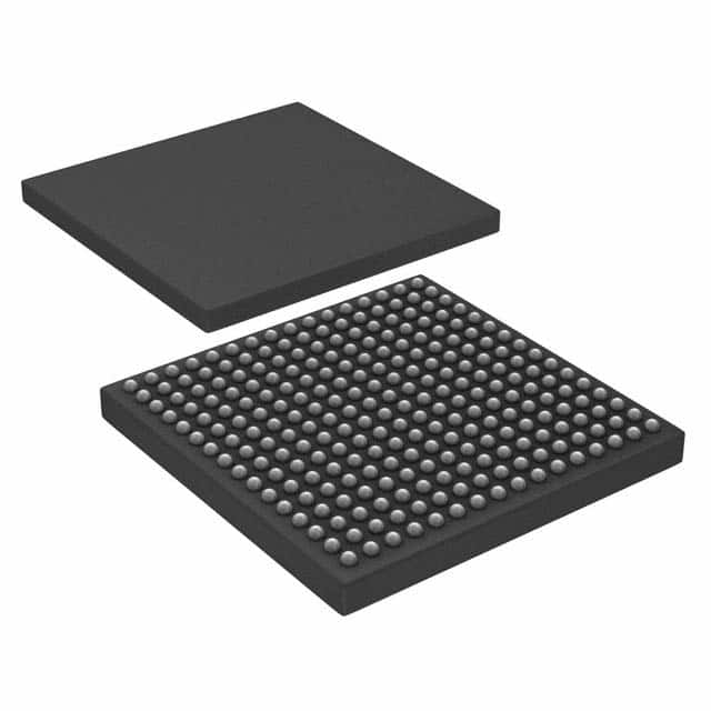
M2S005-1VFG256I comes in a 256-pin Fine-Pitch Ball Grid Array (FBGA) package.
Essence
The essence of M2S005-1VFG256I lies in its ability to provide a customizable hardware platform that allows users to implement their own digital designs efficiently.
Packaging/Quantity
This product is typically packaged individually and is available in various quantities depending on the customer's requirements.
Specifications
- FPGA Family: M2S Series
- Logic Cells: 5,000
- Block RAM: 360 Kbits
- Maximum Frequency: 400 MHz
- I/O Pins: 256
- Operating Voltage: 1.2V
- Configuration Memory: Flash-based
Detailed Pin Configuration
The pin configuration of M2S005-1VFG256I is as follows:
| Pin Number | Pin Name | Description | |------------|----------|-------------| | 1 | VCCINT | Power Supply (Internal) | | 2 | GND | Ground | | 3 | IO0 | General Purpose I/O Pin 0 | | ... | ... | ... | | 256 | IO255 | General Purpose I/O Pin 255 |
Functional Features
- High-speed serial transceivers
- Clock management resources
- Embedded memory blocks
- Programmable I/O standards
- Built-in DSP blocks for signal processing
- On-chip configuration memory
- Support for partial reconfiguration
Advantages and Disadvantages
Advantages
- Flexibility to implement custom digital designs
- Fast processing speed
- Low power consumption
- Large number of logic cells and memory resources
- Support for various communication protocols
Disadvantages
- Steep learning curve for beginners
- Higher cost compared to fixed-function integrated circuits
- Limited availability of alternative models
Working Principles
M2S005-1VFG256I operates based on the principles of reconfigurable computing. It consists of a matrix of programmable logic elements interconnected by configurable routing resources. The user can program the FPGA to implement desired digital logic functions by configuring the interconnections and functionality of these logic elements.
Detailed Application Field Plans
M2S005-1VFG256I finds applications in various fields, including but not limited to: - Telecommunications - Industrial automation - Medical devices - Aerospace and defense - Automotive electronics - Consumer electronics
Detailed and Complete Alternative Models
While M2S005-1VFG256I is a highly capable FPGA, there are alternative models available from different manufacturers that offer similar functionalities. Some notable alternatives include: - Xilinx Spartan-6 XC6SLX9 - Intel Cyclone IV EP4CE6 - Lattice iCE40UP5K
These alternative models provide varying levels of performance, capacity, and price points, allowing users to choose the most suitable option for their specific requirements.
Word count: 525 words
Sebutkan 10 pertanyaan dan jawaban umum terkait penerapan M2S005-1VFG256I dalam solusi teknis
Sure! Here are 10 common questions and answers related to the application of M2S005-1VFG256I in technical solutions:
Q1: What is M2S005-1VFG256I? A1: M2S005-1VFG256I is a specific model of field-programmable gate array (FPGA) manufactured by Microsemi Corporation.
Q2: What are the key features of M2S005-1VFG256I? A2: Some key features of M2S005-1VFG256I include 5,120 logic elements, 128 Kbits of embedded memory, 4 PLLs, and support for various I/O standards.
Q3: What applications can M2S005-1VFG256I be used for? A3: M2S005-1VFG256I can be used in a wide range of applications such as industrial automation, telecommunications, automotive systems, medical devices, and more.
Q4: How can I program M2S005-1VFG256I? A4: M2S005-1VFG256I can be programmed using industry-standard hardware description languages (HDLs) like VHDL or Verilog. Programming tools provided by Microsemi can be used for synthesis, simulation, and programming.
Q5: What voltage levels does M2S005-1VFG256I support? A5: M2S005-1VFG256I supports both 3.3V and 1.2V voltage levels for different parts of the chip.
Q6: Can M2S005-1VFG256I interface with other components or devices? A6: Yes, M2S005-1VFG256I has a variety of I/O standards and interfaces including LVCMOS, LVTTL, LVDS, and more, making it compatible with various components and devices.
Q7: What is the power consumption of M2S005-1VFG256I? A7: The power consumption of M2S005-1VFG256I depends on the specific design and usage. It is recommended to refer to the datasheet or consult Microsemi for detailed power consumption information.
Q8: Can M2S005-1VFG256I be used in safety-critical applications? A8: Yes, M2S005-1VFG256I can be used in safety-critical applications. However, it is important to follow industry best practices and perform thorough verification and validation to ensure compliance with safety standards.
Q9: Are there any development boards available for M2S005-1VFG256I? A9: Yes, Microsemi offers development boards specifically designed for M2S005-1VFG256I, which provide a convenient platform for prototyping and testing.
Q10: Where can I find technical documentation and support for M2S005-1VFG256I? A10: Technical documentation, including datasheets, user guides, and application notes, can be found on Microsemi's website. Additionally, Microsemi provides customer support through their online resources, forums, and direct contact channels.