

Lihat spesifikasi untuk detail produk.
A3PN020-QNG68I
Product Overview
Category
The A3PN020-QNG68I belongs to the category of programmable logic devices (PLDs).
Use
This product is primarily used in digital circuit design and implementation. It provides a flexible and customizable solution for various applications.
Characteristics
- Programmable: The A3PN020-QNG68I can be programmed to perform specific functions based on user requirements.
- High Integration: It offers a high level of integration, allowing for complex designs to be implemented on a single device.
- Versatile: This PLD supports a wide range of applications due to its programmability.
- Low Power Consumption: The A3PN020-QNG68I is designed to operate efficiently with low power consumption.
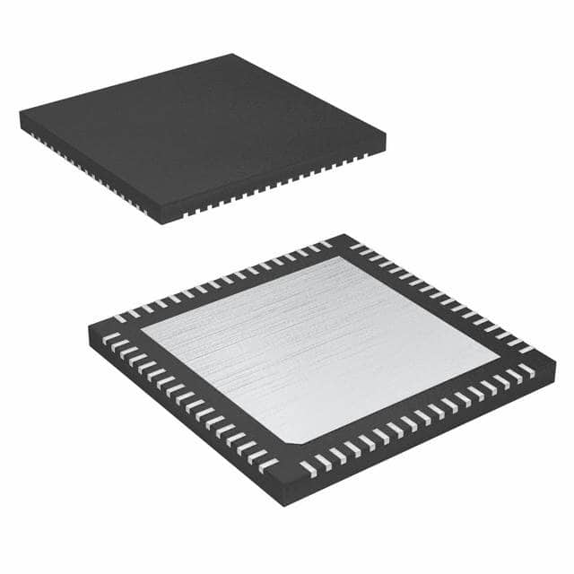
Package
The A3PN020-QNG68I comes in a Quad Flat No-Lead (QFN) package.
Essence
The essence of this product lies in its ability to provide a reconfigurable hardware platform that enables users to implement custom digital circuits.
Packaging/Quantity
The A3PN020-QNG68I is typically packaged individually and is available in quantities suitable for both prototyping and production purposes.
Specifications
- Model: A3PN020-QNG68I
- Logic Cells: 20,000
- I/O Pins: 68
- Operating Voltage: 1.2V
- Speed Grade: Standard
- Package Type: QFN
- Temperature Range: -40°C to +85°C
Detailed Pin Configuration
The A3PN020-QNG68I has a total of 68 I/O pins. The pin configuration is as follows:
(Pin Number) (Pin Name) 1. VCCIO 2. GND 3. IO0 4. IO1 5. IO2 6. IO3 7. IO4 8. IO5 9. IO6 10. IO7 11. IO8 12. IO9 13. IO10 14. IO11 15. IO12 16. IO13 17. IO14 18. IO15 19. IO16 20. IO17 21. IO18 22. IO19 23. IO20 24. IO21 25. IO22 26. IO23 27. IO24 28. IO25 29. IO26 30. IO27 31. IO28 32. IO29 33. IO30 34. IO31 35. IO32 36. IO33 37. IO34 38. IO35 39. IO36 40. IO37 41. IO38 42. IO39 43. IO40 44. IO41 45. IO42 46. IO43 47. IO44 48. IO45 49. IO46 50. IO47 51. IO48 52. IO49 53. IO50 54. IO51 55. IO52 56. IO53 57. IO54 58. IO55 59. IO56 60. IO57 61. IO58 62. IO59 63. IO60 64. IO61 65. IO62 66. IO63 67. IO64 68. IO65
Functional Features
- Reconfigurable Logic: The A3PN020-QNG68I allows users to modify the logic functions and interconnections within the device, providing flexibility in circuit design.
- Embedded Memory: This PLD includes embedded memory blocks that can be used for data storage or as lookup tables.
- Clock Management: The device supports clock management features, allowing for precise timing control in digital circuits.
- I/O Flexibility: With 68 I/O pins, the A3PN020-QNG68I offers ample flexibility for interfacing with external devices.
Advantages and Disadvantages
Advantages
- Customizability: The A3PN020-QNG68I enables users to create tailored digital circuits to meet specific requirements.
- Cost-Effective: By using a single programmable device, costs associated with manufacturing and inventory management can be reduced.
- Time-Saving: The reconfigurable nature of this PLD eliminates the need for redesigning and fabricating custom integrated circuits.
Disadvantages
- Learning Curve: Utilizing programmable logic devices requires knowledge of hardware description languages and digital circuit design principles.
- Limited Performance: Compared to application-specific integrated circuits (ASICs), PLDs may have lower performance capabilities in certain applications.
Working Principles
The A3PN020-QNG68I operates based on the principles of field-programmable gate arrays (FPGAs). It consists of configurable logic blocks (CLBs) interconnected through programmable routing resources. Users can program the
Sebutkan 10 pertanyaan dan jawaban umum terkait penerapan A3PN020-QNG68I dalam solusi teknis
Sure! Here are 10 common questions and answers related to the application of A3PN020-QNG68I in technical solutions:
Q: What is A3PN020-QNG68I? A: A3PN020-QNG68I is a specific model of field-programmable gate array (FPGA) manufactured by Microsemi.
Q: What are the key features of A3PN020-QNG68I? A: Some key features include 20,000 logic elements, 1,152 Kbits of embedded memory, and a QFN68 package.
Q: What are the typical applications for A3PN020-QNG68I? A: A3PN020-QNG68I is commonly used in various technical solutions such as industrial automation, telecommunications, automotive systems, and medical devices.
Q: How can I program A3PN020-QNG68I? A: You can program A3PN020-QNG68I using hardware description languages (HDLs) like VHDL or Verilog, and then use a programming tool provided by Microsemi to load the bitstream onto the FPGA.
Q: Can A3PN020-QNG68I be reprogrammed after deployment? A: Yes, A3PN020-QNG68I is a reprogrammable FPGA, allowing you to modify its functionality even after it has been deployed in a system.
Q: What kind of power supply does A3PN020-QNG68I require? A: A3PN020-QNG68I typically requires a single power supply voltage of 3.3V.
Q: Does A3PN020-QNG68I support external memory interfaces? A: Yes, A3PN020-QNG68I supports various external memory interfaces such as DDR, SDRAM, and Flash.
Q: Can A3PN020-QNG68I interface with other components or devices? A: Yes, A3PN020-QNG68I can interface with other components or devices through its GPIO pins, serial communication protocols like SPI or I2C, and standard bus interfaces like UART or CAN.
Q: What kind of development tools are available for A3PN020-QNG68I? A: Microsemi provides a range of development tools including design software, programming tools, and evaluation boards to facilitate the development process.
Q: Are there any application notes or reference designs available for A3PN020-QNG68I? A: Yes, Microsemi provides application notes, reference designs, and technical documentation to help users understand and implement A3PN020-QNG68I in their technical solutions.
Please note that the specific details and answers may vary depending on the manufacturer's documentation and guidelines for A3PN020-QNG68I.