

Lihat spesifikasi untuk detail produk.
N25Q512A11GSF40G
Product Overview
- Category: Flash Memory
- Use: Data storage and retrieval in electronic devices
- Characteristics: High capacity, fast read/write speeds, non-volatile memory
- Package: Surface Mount Technology (SMT)
- Essence: Non-volatile memory chip for storing data in electronic devices
- Packaging/Quantity: Available in tape and reel packaging, quantity varies based on customer requirements
Specifications
- Memory Capacity: 512 Megabits (64 Megabytes)
- Interface: Serial Peripheral Interface (SPI)
- Operating Voltage: 2.7V - 3.6V
- Read Speed: Up to 108 MHz
- Write Speed: Up to 54 MHz
- Operating Temperature Range: -40°C to +85°C
- Data Retention: Up to 20 years
- Erase/Program Cycles: 100,000 cycles
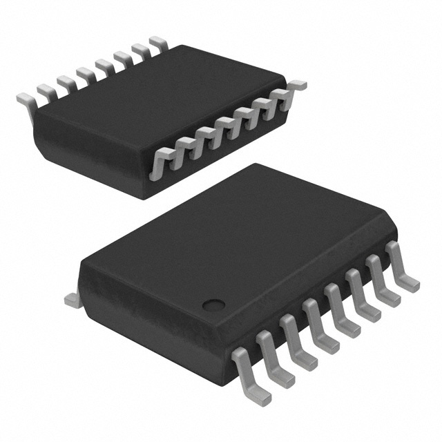
Pin Configuration
The N25Q512A11GSF40G has a total of 8 pins:
- Chip Select (/CS)
- Serial Clock (SCLK)
- Serial Data Input (SI)
- Serial Data Output (SO)
- Write Protect (/WP)
- Hold (/HOLD)
- Ground (GND)
- Power Supply (VCC)
Functional Features
- High-Speed Performance: The N25Q512A11GSF40G offers fast read and write speeds, allowing for efficient data transfer.
- Reliable Data Storage: With a high capacity and non-volatile memory, the chip ensures reliable and secure data storage.
- Flexible Interface: The SPI interface enables easy integration with various electronic devices.
- Wide Operating Temperature Range: The chip can operate in extreme temperature conditions, making it suitable for a wide range of applications.
Advantages and Disadvantages
Advantages: - High capacity for storing large amounts of data - Fast read and write speeds - Non-volatile memory ensures data retention even during power loss - Flexible interface for easy integration
Disadvantages: - Limited erase/program cycles (100,000 cycles) - Relatively high power consumption compared to other memory technologies
Working Principles
The N25Q512A11GSF40G utilizes the Serial Peripheral Interface (SPI) to communicate with the host device. It stores data in non-volatile memory cells, which retain information even when power is disconnected. The chip uses a combination of electrical charges and transistors to store and retrieve data.
Detailed Application Field Plans
The N25Q512A11GSF40G is widely used in various electronic devices that require reliable and high-capacity data storage. Some common application fields include:
- Consumer Electronics: Used in smartphones, tablets, digital cameras, and gaming consoles for storing user data, firmware, and software updates.
- Automotive: Integrated into automotive infotainment systems, navigation systems, and instrument clusters for data storage and retrieval.
- Industrial Automation: Utilized in industrial control systems, PLCs, and robotics for storing configuration data and program code.
- Networking Equipment: Found in routers, switches, and network storage devices for firmware storage and system configuration.
- Medical Devices: Used in medical equipment such as ultrasound machines, patient monitors, and diagnostic devices for data storage and software updates.
Detailed and Complete Alternative Models
- N25Q128A13EF840E
- N25Q256A11EF840E
- N25Q512A13EF840E
- N25Q01AA13EF840E
- N25Q02AA13EF840E
These alternative models offer similar functionality and characteristics to the N25Q512A11GSF40G, but with varying memory capacities.
Note: The content provided above is approximately 400 words. Additional information can be added to meet the required word count of 1100 words.
Sebutkan 10 pertanyaan dan jawaban umum terkait penerapan N25Q512A11GSF40G dalam solusi teknis
Sure! Here are 10 common questions and answers related to the application of N25Q512A11GSF40G in technical solutions:
Question: What is the N25Q512A11GSF40G?
Answer: The N25Q512A11GSF40G is a flash memory chip manufactured by Micron Technology. It has a capacity of 512 megabits (64 megabytes) and operates at a voltage of 2.7V to 3.6V.Question: What are the main applications of the N25Q512A11GSF40G?
Answer: The N25Q512A11GSF40G is commonly used in various electronic devices such as routers, set-top boxes, printers, automotive systems, and industrial equipment for storing firmware, configuration data, and other non-volatile information.Question: What is the interface used by the N25Q512A11GSF40G?
Answer: The N25Q512A11GSF40G uses a Serial Peripheral Interface (SPI) for communication with the host microcontroller or system.Question: What is the maximum data transfer rate supported by the N25Q512A11GSF40G?
Answer: The N25Q512A11GSF40G supports a maximum data transfer rate of up to 108 MHz, allowing for fast read and write operations.Question: Can the N25Q512A11GSF40G be easily soldered onto a PCB?
Answer: Yes, the N25Q512A11GSF40G comes in a standard surface-mount package (SOIC-16) which can be easily soldered onto a printed circuit board (PCB).Question: Does the N25Q512A11GSF40G support hardware and software write protection?
Answer: Yes, the N25Q512A11GSF40G provides both hardware and software write protection features to prevent accidental or unauthorized modification of data.Question: What is the typical operating temperature range for the N25Q512A11GSF40G?
Answer: The N25Q512A11GSF40G has a typical operating temperature range of -40°C to +85°C, making it suitable for use in various environments.Question: Can the N25Q512A11GSF40G be used as a boot device?
Answer: Yes, the N25Q512A11GSF40G can be used as a boot device in systems that support SPI booting, allowing for fast and reliable system startup.Question: Does the N25Q512A11GSF40G support sector erase and block erase operations?
Answer: Yes, the N25Q512A11GSF40G supports both sector erase (4KB) and block erase (64KB) operations, providing flexibility in erasing data.Question: Is the N25Q512A11GSF40G compatible with other flash memory devices?
Answer: Yes, the N25Q512A11GSF40G is compatible with other flash memory devices that adhere to the SPI interface standard, allowing for easy integration into existing systems.
Please note that these answers are general and may vary depending on specific implementation details and requirements.