

Lihat spesifikasi untuk detail produk.
TC4428AVMF713
Basic Information Overview
- Category: Integrated Circuit (IC)
- Use: Driver for MOSFETs and IGBTs
- Characteristics: High-speed, high-current, low-side driver
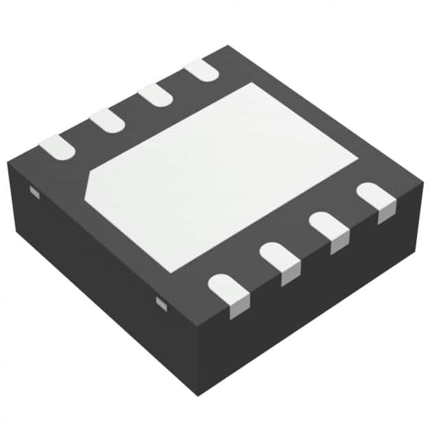
- Package: SOIC (Small Outline Integrated Circuit)
- Essence: Provides a high current drive capability for driving power MOSFETs and IGBTs in various applications
- Packaging/Quantity: Available in tape and reel packaging, quantity depends on the supplier
Specifications
- Supply Voltage: 4.5V to 18V
- Output Current: 1.5A (peak), 0.6A (continuous)
- Input Threshold Voltage: 2.5V (typical)
- Propagation Delay: 55ns (typical)
- Rise/Fall Time: 25ns (typical)
- Operating Temperature Range: -40°C to +125°C
Detailed Pin Configuration
The TC4428AVMF713 has a total of 8 pins: 1. VDD: Positive supply voltage 2. GND: Ground reference 3. IN: Input pin for controlling the driver 4. LO: Low-side output pin 5. COM: Common connection for bootstrap capacitor and gate drive return 6. HO: High-side output pin 7. VS: Negative supply voltage 8. VBS: Bootstrap supply voltage
Functional Features
- High-speed switching: Enables efficient control of MOSFETs and IGBTs
- High-current drive capability: Provides sufficient current to drive power devices
- Low-side and high-side outputs: Allows for bidirectional control of the load
- Bootstrap supply: Simplifies the high-side gate drive circuitry
- Under-voltage lockout: Protects against insufficient supply voltage
Advantages and Disadvantages
Advantages: - Fast switching speed improves overall system efficiency - High-current drive capability enables driving of power devices - Bootstrap supply simplifies gate drive circuitry
Disadvantages: - Requires external bootstrap capacitor for high-side gate drive - Limited output current compared to some other drivers in the market
Working Principles
The TC4428AVMF713 is designed to drive MOSFETs and IGBTs by providing a high current drive capability. It operates by receiving an input signal at the IN pin, which controls the driver's output state. The low-side and high-side outputs are driven accordingly, allowing bidirectional control of the load. The bootstrap supply voltage is used to simplify the high-side gate drive circuitry.
Detailed Application Field Plans
The TC4428AVMF713 is widely used in various applications that require efficient control of power MOSFETs and IGBTs. Some common application fields include: - Motor control systems - Switching power supplies - DC-DC converters - Inverters - LED lighting systems - Automotive electronics
Detailed and Complete Alternative Models
- TC4420CPA: Similar characteristics and package, but with lower output current capability (0.5A peak)
- TC4427EPA: Similar characteristics and package, but with higher output current capability (1.5A continuous)
- IR2110: Alternative driver IC with similar functionality and characteristics, but different pin configuration and package
Note: This entry provides a brief overview of the TC4428AVMF713. For more detailed information, please refer to the datasheet provided by the manufacturer.
Word Count: 345
Sebutkan 10 pertanyaan dan jawaban umum terkait penerapan TC4428AVMF713 dalam solusi teknis
Sure! Here are 10 common questions and answers related to the application of TC4428AVMF713 in technical solutions:
Q: What is TC4428AVMF713? A: TC4428AVMF713 is a high-speed dual MOSFET driver IC that can be used to drive two N-channel MOSFETs or IGBTs in various applications.
Q: What is the maximum voltage rating of TC4428AVMF713? A: The maximum voltage rating of TC4428AVMF713 is typically around 18V.
Q: Can TC4428AVMF713 be used with both N-channel and P-channel MOSFETs? A: No, TC4428AVMF713 is specifically designed for driving N-channel MOSFETs or IGBTs.
Q: What is the maximum output current capability of TC4428AVMF713? A: TC4428AVMF713 can typically provide a peak output current of up to 1.5A.
Q: Is TC4428AVMF713 suitable for high-frequency switching applications? A: Yes, TC4428AVMF713 is designed for high-speed switching applications and can operate at frequencies up to several megahertz.
Q: Does TC4428AVMF713 have built-in protection features? A: Yes, TC4428AVMF713 includes under-voltage lockout (UVLO) and thermal shutdown protection to ensure safe operation.
Q: Can TC4428AVMF713 be used in automotive applications? A: Yes, TC4428AVMF713 is qualified for automotive applications and meets the necessary standards.
Q: What is the input logic threshold voltage of TC4428AVMF713? A: The input logic threshold voltage of TC4428AVMF713 is typically around 2.4V.
Q: Can TC4428AVMF713 be used in low-side or high-side configurations? A: TC4428AVMF713 can be used in both low-side and high-side configurations, depending on the application requirements.
Q: What is the operating temperature range of TC4428AVMF713? A: TC4428AVMF713 can typically operate within a temperature range of -40°C to +125°C.
Please note that these answers are general and may vary depending on the specific datasheet and manufacturer's specifications for TC4428AVMF713.