

Lihat spesifikasi untuk detail produk.
ATF1508AS-7QC100
Product Overview
Category
The ATF1508AS-7QC100 belongs to the category of programmable logic devices (PLDs).
Use
This device is commonly used in digital circuit design and implementation. It provides a flexible and customizable solution for various applications.
Characteristics
- Programmable: The ATF1508AS-7QC100 can be programmed to perform specific functions according to the user's requirements.
- High Integration: It integrates multiple logic gates, flip-flops, and other components into a single chip, reducing the need for external components.
- Versatile: It supports a wide range of applications due to its programmability.
- Low Power Consumption: The ATF1508AS-7QC100 is designed to operate efficiently with low power consumption.
- Fast Operation: It offers high-speed performance, enabling rapid execution of complex logic operations.
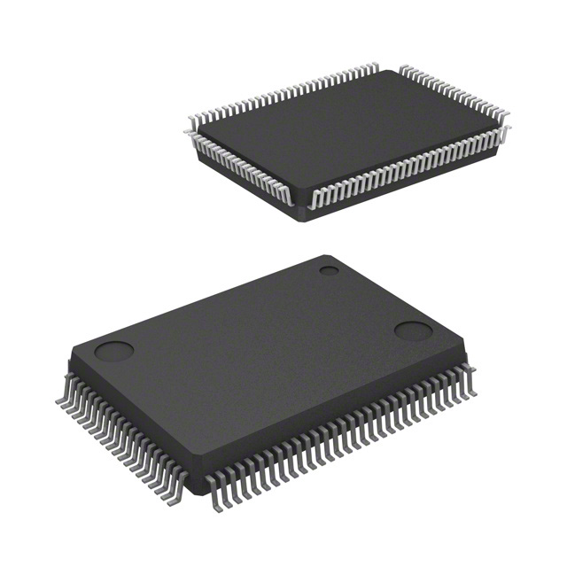
Package
The ATF1508AS-7QC100 is available in a Quad Flat Chip (QFC) package.
Essence
The essence of ATF1508AS-7QC100 lies in its ability to provide reconfigurable logic functions, allowing users to implement custom digital circuits without the need for dedicated hardware.
Packaging/Quantity
The ATF1508AS-7QC100 is typically packaged in reels or tubes, with each containing a specified quantity of devices.
Specifications
- Device Type: ATF1508AS-7QC100
- Logic Cells: 1508
- I/O Pins: 100
- Operating Voltage: 3.3V
- Speed Grade: -7
- Package Type: QFC
Detailed Pin Configuration
The ATF1508AS-7QC100 has a total of 100 pins, which are assigned different functions based on their configuration. The detailed pin configuration is as follows:
(Pin Number) - (Pin Name) - (Function)
1 - VCCIO - Power Supply for I/O Buffers
2 - GND - Ground
3 - TDI - Test Data Input
4 - TMS - Test Mode Select
5 - TCK - Test Clock
6 - TDO - Test Data Output
7 - VCCINT - Internal Power Supply
8 - GND - Ground
...
Functional Features
- Reconfigurable Logic: The ATF1508AS-7QC100 allows users to modify the logic functions it performs, enabling flexibility in circuit design.
- High-Speed Operation: It offers fast operation, making it suitable for applications that require quick response times.
- Low Power Consumption: The device is designed to minimize power consumption, making it energy-efficient.
- Wide Operating Voltage Range: It can operate within a range of 3.3V, providing compatibility with various systems.
Advantages and Disadvantages
Advantages
- Flexibility: The ATF1508AS-7QC100's reconfigurable nature allows for versatile circuit design.
- Integration: Its high integration reduces the need for additional components.
- Customizability: Users can program the device to meet specific requirements.
- Speed: The device operates at high speeds, enabling efficient execution of logic operations.
Disadvantages
- Complexity: Programming and configuring the ATF1508AS-7QC100 may require expertise in digital circuit design.
- Limited Resources: The device has a finite number of logic cells and I/O pins, which may restrict the complexity of designs.
Working Principles
The ATF1508AS-7QC100 utilizes programmable logic elements, such as lookup tables and flip-flops, to implement desired logic functions. These elements are interconnected through configurable routing resources, allowing users to define the desired connections between them. The device's configuration memory stores the user-defined logic functions, which can be modified as needed.
Detailed Application Field Plans
The ATF1508AS-7QC100 finds applications in various fields, including:
- Industrial Automation: It can be used to implement control systems for manufacturing processes.
- Communication Systems: The device enables the design of custom communication protocols and signal processing algorithms.
- Automotive Electronics: It can be utilized in automotive systems for functions like engine control, safety features, and infotainment systems.
- Medical Devices: The ATF1508AS-7QC100 can be employed in medical equipment for data acquisition, signal processing, and control purposes.
- Aerospace and Defense: It finds application in avionics, radar systems, and military equipment for custom logic implementation.
Detailed and Complete Alternative Models
- ATF1508ASV-7QC100
- ATF1508ASL-7QC100
- ATF1508AS-10JC84
- ATF1508AS-15JC84
- ATF1508AS-20JC84
These alternative models offer similar functionality and characteristics to the ATF1508AS-7QC100, providing users with options based on
Sebutkan 10 pertanyaan dan jawaban umum terkait penerapan ATF1508AS-7QC100 dalam solusi teknis
Sure! Here are 10 common questions and answers related to the application of ATF1508AS-7QC100 in technical solutions:
Question: What is ATF1508AS-7QC100?
Answer: ATF1508AS-7QC100 is a specific model of Field-Programmable Gate Array (FPGA) manufactured by Microchip Technology Inc.Question: What are the key features of ATF1508AS-7QC100?
Answer: Some key features of ATF1508AS-7QC100 include 1500 usable gates, 8 macrocells, 8 inputs/outputs, and a maximum operating frequency of 75 MHz.Question: In which technical applications can ATF1508AS-7QC100 be used?
Answer: ATF1508AS-7QC100 can be used in various technical applications such as industrial control systems, communication equipment, automotive electronics, and consumer electronics.Question: How can I program ATF1508AS-7QC100?
Answer: ATF1508AS-7QC100 can be programmed using industry-standard hardware description languages (HDLs) like VHDL or Verilog, along with appropriate programming tools provided by Microchip.Question: Can ATF1508AS-7QC100 be reprogrammed after initial programming?
Answer: No, ATF1508AS-7QC100 is a one-time programmable (OTP) device, meaning it cannot be reprogrammed once it has been programmed.Question: What is the power supply voltage range for ATF1508AS-7QC100?
Answer: The recommended power supply voltage range for ATF1508AS-7QC100 is typically between 4.75V and 5.25V.Question: Does ATF1508AS-7QC100 support external memory interfaces?
Answer: Yes, ATF1508AS-7QC100 supports external memory interfaces such as SRAM, PROM, and EPROM.Question: What is the maximum number of I/O pins supported by ATF1508AS-7QC100?
Answer: ATF1508AS-7QC100 has a total of 8 input/output (I/O) pins available for use in your technical solution.Question: Can ATF1508AS-7QC100 operate in harsh environmental conditions?
Answer: Yes, ATF1508AS-7QC100 is designed to operate reliably in a wide range of temperatures and can withstand harsh environmental conditions.Question: Are there any specific design considerations when using ATF1508AS-7QC100?
Answer: Yes, it is important to carefully review the datasheet and application notes provided by Microchip to ensure proper design considerations such as power supply decoupling, signal integrity, and thermal management are taken into account.
Please note that these answers are general and may vary depending on the specific requirements and documentation provided by Microchip for ATF1508AS-7QC100.