

Lihat spesifikasi untuk detail produk.
ATF1504ASL-25AU100
Product Overview
Category
The ATF1504ASL-25AU100 belongs to the category of programmable logic devices (PLDs).
Use
This device is primarily used for digital circuit design and implementation. It offers a flexible and customizable solution for various applications.
Characteristics
- Programmable: The ATF1504ASL-25AU100 can be programmed to perform specific functions based on user requirements.
- High Integration: It integrates multiple logic gates, flip-flops, and other components into a single chip.
- Versatile: This PLD supports a wide range of applications due to its programmability.
- Low Power Consumption: The ATF1504ASL-25AU100 is designed to operate efficiently with minimal power consumption.
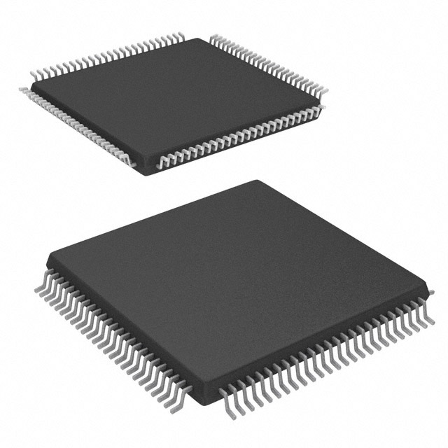
Package
The ATF1504ASL-25AU100 is available in a small form factor package, which ensures easy integration into electronic circuits.
Essence
The essence of this product lies in its ability to provide a reconfigurable logic solution that can be tailored to meet specific design needs.
Packaging/Quantity
The ATF1504ASL-25AU100 is typically packaged in trays or tubes, with each package containing a specified quantity of devices.
Specifications
- Model: ATF1504ASL-25AU100
- Technology: Advanced CMOS
- Speed Grade: 25MHz
- Operating Voltage: 3.3V
- I/O Pins: 100
- Logic Cells: 1500
- Memory: 64K bits
- Package Type: TQFP
Detailed Pin Configuration
The ATF1504ASL-25AU100 has a total of 100 pins, each serving a specific purpose. The pin configuration is as follows:
(Pin Number) - (Pin Name) 1 - VCCIO 2 - GND 3 - IO1 4 - IO2 5 - IO3 ... 100 - IO100
Functional Features
- Reconfigurable Logic: The ATF1504ASL-25AU100 can be programmed to implement various logic functions, allowing for flexibility in circuit design.
- High-Speed Operation: With a speed grade of 25MHz, this PLD can handle complex digital operations efficiently.
- I/O Flexibility: The device offers 100 I/O pins, providing ample connectivity options for interfacing with other components.
- Low Power Consumption: The ATF1504ASL-25AU100 is designed to operate with minimal power consumption, making it suitable for battery-powered applications.
Advantages and Disadvantages
Advantages
- Customizability: The ability to program the device according to specific requirements allows for highly tailored solutions.
- Integration: The ATF1504ASL-25AU100 integrates multiple logic components into a single chip, reducing the need for additional discrete components.
- Versatility: This PLD supports a wide range of applications due to its programmability.
Disadvantages
- Learning Curve: Utilizing the full potential of the ATF1504ASL-25AU100 may require a learning curve for users unfamiliar with programmable logic devices.
- Limited Resources: The device has a finite number of logic cells and I/O pins, which may restrict the complexity of designs that can be implemented.
Working Principles
The ATF1504ASL-25AU100 operates based on the principles of reconfigurable logic. It consists of an array of logic cells that can be interconnected and programmed to perform desired functions. These logic cells can be configured using hardware description languages or dedicated software tools provided by the manufacturer.
Detailed Application Field Plans
The ATF1504ASL-25AU100 finds applications in various fields, including:
- Industrial Automation: It can be used to implement control systems for manufacturing processes, robotics, and machinery.
- Communications: The device can be utilized in networking equipment, such as routers and switches, to handle data processing and routing.
- Automotive Electronics: It can be employed in automotive systems for functions like engine control, driver assistance, and infotainment.
- Consumer Electronics: The ATF1504ASL-25AU100 can be integrated into devices like smart TVs, gaming consoles, and home automation systems.
Detailed and Complete Alternative Models
- ATF1508ASL-25AU100: Similar to the ATF1504ASL-25AU100, but with higher logic capacity and more I/O pins.
- ATF2500C-20PU: A different PLD model with enhanced performance and larger memory capacity.
- XC9572XL-10VQG44C: An alternative programmable logic device from a different manufacturer, offering similar features and capabilities.
These alternative models provide options for users with varying requirements and design constraints.
Word count: 570 words
Sebutkan 10 pertanyaan dan jawaban umum terkait penerapan ATF1504ASL-25AU100 dalam solusi teknis
Sure! Here are 10 common questions and answers related to the application of ATF1504ASL-25AU100 in technical solutions:
Q: What is ATF1504ASL-25AU100? A: ATF1504ASL-25AU100 is a specific model of Field-Programmable Gate Array (FPGA) manufactured by Microchip Technology Inc.
Q: What are the key features of ATF1504ASL-25AU100? A: Some key features of ATF1504ASL-25AU100 include 1500 usable gates, 25ns maximum propagation delay, and 100MHz maximum operating frequency.
Q: In what applications can ATF1504ASL-25AU100 be used? A: ATF1504ASL-25AU100 can be used in various applications such as industrial automation, telecommunications, automotive electronics, and consumer electronics.
Q: How can I program ATF1504ASL-25AU100? A: ATF1504ASL-25AU100 can be programmed using hardware description languages (HDLs) like VHDL or Verilog, along with appropriate development tools provided by the manufacturer.
Q: Can ATF1504ASL-25AU100 be reprogrammed after initial programming? A: No, ATF1504ASL-25AU100 is a one-time programmable (OTP) device, meaning it cannot be reprogrammed once it has been programmed.
Q: What voltage levels does ATF1504ASL-25AU100 support? A: ATF1504ASL-25AU100 supports both 3.3V and 5V voltage levels, making it compatible with a wide range of digital systems.
Q: Does ATF1504ASL-25AU100 have any built-in memory? A: No, ATF1504ASL-25AU100 does not have any built-in memory. It is a pure logic device that requires external memory components if needed.
Q: What is the power consumption of ATF1504ASL-25AU100? A: The power consumption of ATF1504ASL-25AU100 depends on the specific design and usage scenario. It is recommended to refer to the datasheet for detailed power specifications.
Q: Can ATF1504ASL-25AU100 interface with other digital components or microcontrollers? A: Yes, ATF1504ASL-25AU100 can interface with other digital components or microcontrollers using standard communication protocols such as SPI, I2C, UART, etc.
Q: Are there any application notes or reference designs available for ATF1504ASL-25AU100? A: Yes, Microchip Technology Inc. provides application notes, reference designs, and technical documentation on their website, which can be helpful in designing solutions using ATF1504ASL-25AU100.
Please note that the answers provided here are general and may vary depending on the specific requirements and implementation details of your technical solution.