

Lihat spesifikasi untuk detail produk.
ATF1504AS-10JI84
Product Overview
Category
ATF1504AS-10JI84 belongs to the category of programmable logic devices (PLDs).
Use
It is commonly used in digital circuit design and implementation, providing flexibility and reconfigurability.
Characteristics
- Programmable: The ATF1504AS-10JI84 can be programmed to perform various logic functions.
- High Integration: It offers a high level of integration, allowing for complex designs in a single device.
- Reconfigurable: The device can be reprogrammed multiple times, enabling design changes without hardware modifications.
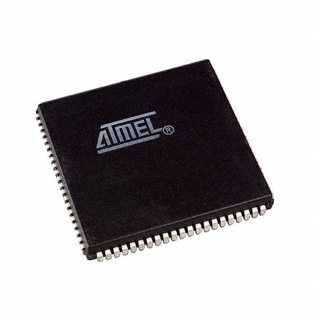
Package
The ATF1504AS-10JI84 comes in a 84-pin J-leaded chip carrier (JIC) package.
Essence
The essence of ATF1504AS-10JI84 lies in its ability to provide a versatile and customizable solution for digital circuit design.
Packaging/Quantity
The ATF1504AS-10JI84 is typically packaged individually and is available in various quantities depending on the supplier.
Specifications
- Device Type: Programmable Logic Device (PLD)
- Family: ATF1504AS
- Speed Grade: -10
- Package Type: 84-pin JIC
- Operating Temperature Range: -40°C to +85°C
- Supply Voltage: 3.3V
- Number of I/O Pins: 68
- Maximum Gates: 1500
- Programmable Logic Cells: 84
Detailed Pin Configuration
The ATF1504AS-10JI84 has a total of 84 pins. The pin configuration is as follows:
(Pin Number - Pin Name - Description) 1 - VCCIO - I/O Power Supply 2 - GND - Ground 3 - TCK - Test Clock Input 4 - TMS - Test Mode Select 5 - TDI - Test Data Input 6 - TDO - Test Data Output 7 - GND - Ground 8 - VCCIO - I/O Power Supply 9 - IO1 - General Purpose I/O Pin 1 10 - IO2 - General Purpose I/O Pin 2 ... 84 - GND - Ground
Functional Features
- High-Speed Operation: The ATF1504AS-10JI84 operates at high clock frequencies, enabling rapid data processing.
- Flexible I/O Configuration: It offers a wide range of I/O options, allowing for versatile interfacing with external devices.
- On-Chip Memory: The device includes embedded memory blocks for storing configuration data and user-defined look-up tables.
- JTAG Support: It supports Joint Test Action Group (JTAG) interface for programming and debugging.
Advantages and Disadvantages
Advantages
- Flexibility: The ATF1504AS-10JI84 provides flexibility in designing digital circuits, accommodating various logic functions.
- Reconfigurability: Its ability to be reprogrammed multiple times allows for design changes without hardware modifications.
- Integration: The high level of integration reduces the need for additional components, simplifying circuit design.
Disadvantages
- Complexity: Programming and configuring the ATF1504AS-10JI84 can be complex, requiring expertise in digital circuit design.
- Limited Resources: The device has a finite number of gates and I/O pins, which may restrict the complexity of designs.
Working Principles
The ATF1504AS-10JI84 utilizes programmable logic cells and interconnect resources to implement desired logic functions. These logic cells can be interconnected using programmable routing resources, allowing for the creation of complex digital circuits. The device is programmed using specialized software tools that generate a configuration file, which is then loaded onto the ATF1504AS-10JI84.
Detailed Application Field Plans
The ATF1504AS-10JI84 finds applications in various fields, including: - Embedded Systems: It can be used to implement control and interface logic in embedded systems. - Communication Systems: The device can be utilized for protocol conversion, signal processing, and data manipulation in communication systems. - Industrial Automation: It enables the implementation of custom logic for automation and control in industrial environments. - Consumer Electronics: The ATF1504AS-10JI84 can be employed in consumer electronics devices for custom functionality and interface control.
Detailed and Complete Alternative Models
Some alternative models to ATF1504AS-10JI84 include: - ATF1504AS-15JI84 - ATF1504AS-20JI84 - ATF1504AS-25JI84 - ATF1504AS-30JI84
These models offer similar functionality but may differ in speed grade or other specifications.
Word count: 570 words
Sebutkan 10 pertanyaan dan jawaban umum terkait penerapan ATF1504AS-10JI84 dalam solusi teknis
Sure! Here are 10 common questions and answers related to the application of ATF1504AS-10JI84 in technical solutions:
Q: What is ATF1504AS-10JI84? A: ATF1504AS-10JI84 is a specific model of Field-Programmable Gate Array (FPGA) manufactured by Microchip Technology Inc.
Q: What are the key features of ATF1504AS-10JI84? A: Some key features of ATF1504AS-10JI84 include 1500 usable gates, 84-pin PLCC package, 10ns maximum propagation delay, and 5V voltage compatibility.
Q: What are the typical applications of ATF1504AS-10JI84? A: ATF1504AS-10JI84 can be used in various applications such as industrial control systems, automotive electronics, telecommunications, and consumer electronics.
Q: How can I program ATF1504AS-10JI84? A: ATF1504AS-10JI84 can be programmed using industry-standard hardware description languages (HDL) like VHDL or Verilog, along with appropriate programming tools provided by the manufacturer.
Q: Can ATF1504AS-10JI84 be reprogrammed after initial programming? A: No, ATF1504AS-10JI84 is a one-time programmable FPGA and cannot be reprogrammed once it has been programmed.
Q: What is the power supply requirement for ATF1504AS-10JI84? A: ATF1504AS-10JI84 requires a 5V power supply for proper operation.
Q: Does ATF1504AS-10JI84 support external memory interfaces? A: Yes, ATF1504AS-10JI84 supports external memory interfaces such as SRAM, SDRAM, and Flash memory.
Q: Can ATF1504AS-10JI84 interface with other digital components or microcontrollers? A: Yes, ATF1504AS-10JI84 can interface with other digital components or microcontrollers through standard communication protocols like SPI, I2C, UART, or GPIO pins.
Q: What is the maximum operating frequency of ATF1504AS-10JI84? A: The maximum operating frequency of ATF1504AS-10JI84 is typically around 100 MHz, but it may vary depending on the specific design and implementation.
Q: Are there any development boards or evaluation kits available for ATF1504AS-10JI84? A: Yes, Microchip Technology Inc. provides development boards and evaluation kits specifically designed for ATF1504AS-10JI84, which can help in prototyping and testing applications using this FPGA.
Please note that the answers provided here are general and may vary based on specific requirements and documentation provided by the manufacturer.