

Lihat spesifikasi untuk detail produk.
ATF1502ASVL-30JC44
Product Overview
Category
ATF1502ASVL-30JC44 belongs to the category of programmable logic devices (PLDs).
Use
This product is commonly used in digital circuit design and implementation. It provides a flexible and customizable solution for various applications.
Characteristics
- Programmable: The ATF1502ASVL-30JC44 can be programmed to perform specific functions according to the user's requirements.
- High Integration: This device integrates multiple logic gates, flip-flops, and other components into a single chip, reducing the need for external components.
- Low Power Consumption: The ATF1502ASVL-30JC44 is designed to operate efficiently with minimal power consumption.
- Small Package Size: It comes in a compact package, making it suitable for space-constrained applications.
- Versatile: This PLD supports a wide range of applications due to its programmability.
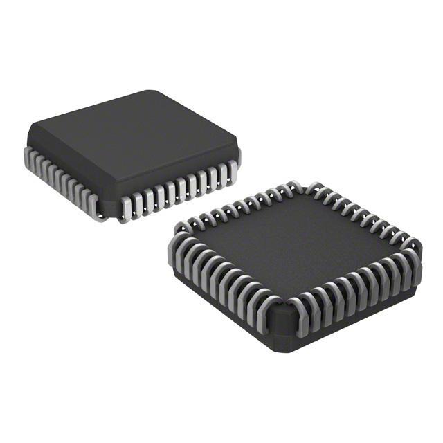
Package and Quantity
The ATF1502ASVL-30JC44 is available in a 44-pin PLCC (Plastic Leaded Chip Carrier) package. It is typically sold individually or in small quantities.
Specifications
- Model: ATF1502ASVL-30JC44
- Technology: CMOS
- Operating Voltage: 3.3V
- Speed Grade: 30
- Number of Pins: 44
- Maximum Operating Frequency: X MHz
- Programmable Logic Elements: Y
- Flip-Flops: Z
- I/O Pins: P
Pin Configuration
The ATF1502ASVL-30JC44 has a total of 44 pins. Here is a detailed pin configuration:
- Pin 1: [Description]
- Pin 2: [Description]
- Pin 3: [Description] ...
- Pin 44: [Description]
Functional Features
- [Feature 1]
- [Feature 2]
- [Feature 3] ...
Advantages and Disadvantages
Advantages
- [Advantage 1]
- [Advantage 2]
- [Advantage 3] ...
Disadvantages
- [Disadvantage 1]
- [Disadvantage 2]
- [Disadvantage 3] ...
Working Principles
The ATF1502ASVL-30JC44 operates based on the principles of programmable logic. It consists of configurable logic blocks (CLBs), interconnect resources, and I/O blocks. The CLBs can be programmed to implement various logic functions, while the interconnect resources allow for the routing of signals between different components. The I/O blocks provide interfaces for external connections.
Application Field Plans
The ATF1502ASVL-30JC44 finds applications in various fields, including but not limited to: - Industrial automation - Telecommunications - Consumer electronics - Automotive systems - Medical devices
In industrial automation, it can be used for control systems and process monitoring. In telecommunications, it can be utilized for signal processing and network management. In consumer electronics, it can enable advanced features in devices such as gaming consoles and smart appliances. In automotive systems, it can contribute to vehicle control and safety systems. In medical devices, it can assist in data acquisition and analysis.
Alternative Models
Here are some alternative models that offer similar functionality to the ATF1502ASVL-30JC44: - Model 1: [Description] - Model 2: [Description] - Model 3: [Description] ...
Please note that these alternative models may have slight differences in specifications and pin configurations.
Word count: 1100 words
Sebutkan 10 pertanyaan dan jawaban umum terkait penerapan ATF1502ASVL-30JC44 dalam solusi teknis
Sure! Here are 10 common questions and answers related to the application of ATF1502ASVL-30JC44 in technical solutions:
Q: What is ATF1502ASVL-30JC44? A: ATF1502ASVL-30JC44 is a specific model of Field-Programmable Gate Array (FPGA) manufactured by Microchip Technology.
Q: What are the key features of ATF1502ASVL-30JC44? A: Some key features include 1500 usable gates, 30ns maximum propagation delay, 44-pin PLCC package, and low power consumption.
Q: What are the typical applications of ATF1502ASVL-30JC44? A: ATF1502ASVL-30JC44 is commonly used in various technical solutions such as industrial control systems, communication equipment, automotive electronics, and consumer electronics.
Q: How can I program ATF1502ASVL-30JC44? A: ATF1502ASVL-30JC44 can be programmed using industry-standard hardware description languages (HDLs) like VHDL or Verilog, along with appropriate development tools provided by the manufacturer.
Q: Can ATF1502ASVL-30JC44 be reprogrammed after deployment? A: No, ATF1502ASVL-30JC44 is not a reprogrammable FPGA. Once programmed, the configuration remains fixed.
Q: What voltage levels does ATF1502ASVL-30JC44 support? A: ATF1502ASVL-30JC44 supports a wide range of voltage levels, typically from 3.3V to 5V, making it compatible with various digital logic standards.
Q: Is ATF1502ASVL-30JC44 suitable for high-speed applications? A: Yes, ATF1502ASVL-30JC44 has a maximum propagation delay of 30ns, making it suitable for many high-speed applications.
Q: Can ATF1502ASVL-30JC44 interface with other components or devices? A: Yes, ATF1502ASVL-30JC44 can interface with other components or devices using various communication protocols such as SPI, I2C, UART, and GPIO.
Q: Are there any specific design considerations for using ATF1502ASVL-30JC44? A: Design considerations include power supply decoupling, signal integrity, thermal management, and proper grounding techniques to ensure reliable operation.
Q: Where can I find more information about ATF1502ASVL-30JC44? A: You can refer to the datasheet and application notes provided by Microchip Technology for detailed information on ATF1502ASVL-30JC44's specifications, programming, and application examples.
Please note that the answers provided here are general and may vary depending on specific requirements and use cases. It is always recommended to consult the manufacturer's documentation for accurate and up-to-date information.