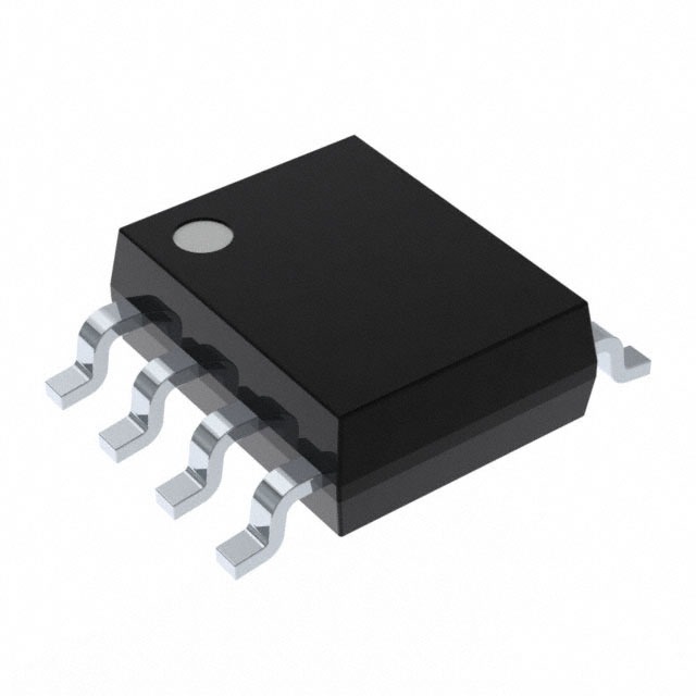
Lihat spesifikasi untuk detail produk.

MAX9077ESA+T
Product Overview
- Category: Integrated Circuit (IC)
- Use: Amplifier
- Characteristics: Low-power, high-speed, rail-to-rail output, single-supply operation
- Package: 8-pin SOIC (Small Outline Integrated Circuit)
- Essence: The MAX9077ESA+T is a low-power, high-speed amplifier designed for single-supply applications.
- Packaging/Quantity: Available in tape and reel packaging with 2500 units per reel.
Specifications
- Supply Voltage: 2.7V to 5.5V
- Input Offset Voltage: ±1mV (maximum)
- Gain Bandwidth Product: 100MHz (typical)
- Slew Rate: 90V/µs (typical)
- Input Bias Current: 1pA (typical)
- Operating Temperature Range: -40°C to +85°C
Pin Configuration
The MAX9077ESA+T has the following pin configuration:
```
| | --| IN- OUT |-- Pin 1: IN- --| IN+ VCC |-- Pin 2: IN+ --| GND NC |-- Pin 3: GND --| NC NC |-- Pin 4: Not Connected --| NC NC |-- Pin 5: Not Connected --| NC VEE |-- Pin 6: VEE --| NC NC |-- Pin 7: Not Connected --| NC NC |-- Pin 8: Not Connected |___________| ```
Functional Features
- Low-power consumption makes it suitable for battery-powered applications.
- High-speed performance enables accurate signal amplification in time-critical applications.
- Rail-to-rail output allows for maximum signal swing.
- Single-supply operation simplifies circuit design and reduces component count.
Advantages
- Low input offset voltage ensures accurate amplification of small signals.
- Wide operating temperature range makes it suitable for various environments.
- Small package size saves board space in compact designs.
- High gain bandwidth product enables amplification of high-frequency signals.
Disadvantages
- Limited number of pins may restrict the number of external components that can be connected.
- Not suitable for applications requiring high power amplification.
Working Principles
The MAX9077ESA+T is a voltage amplifier that operates on a single supply voltage. It uses a differential input stage to amplify the voltage difference between the IN+ and IN- pins. The amplified signal is then passed through an output stage, which provides a rail-to-rail output swing. The amplifier operates with low power consumption and is designed to work in a wide temperature range.
Detailed Application Field Plans
The MAX9077ESA+T is commonly used in the following applications:
- Portable audio devices
- Sensor signal conditioning
- Medical instrumentation
- Communication systems
- Industrial control systems
Alternative Models
Here are some alternative models that offer similar functionality:
- AD8605: Low-power, rail-to-rail input/output amplifier
- LT1677: Precision, low-noise, rail-to-rail output amplifier
- MCP6002: Low-power, rail-to-rail input/output operational amplifier
These alternative models can be considered based on specific application requirements and design constraints.
In conclusion, the MAX9077ESA+T is a versatile amplifier IC that offers low-power, high-speed performance with rail-to-rail output capability. Its small package size and wide operating temperature range make it suitable for various applications in different industries. However, designers should consider alternative models depending on their specific needs.
Sebutkan 10 pertanyaan dan jawaban umum terkait penerapan MAX9077ESA+T dalam solusi teknis
Sure! Here are 10 common questions and answers related to the application of MAX9077ESA+T in technical solutions:
Q: What is the MAX9077ESA+T? A: The MAX9077ESA+T is a high-speed, low-power operational amplifier (op-amp) designed for use in various technical applications.
Q: What is the supply voltage range for the MAX9077ESA+T? A: The supply voltage range for the MAX9077ESA+T is typically between +2.7V and +5.5V.
Q: What is the maximum operating temperature for the MAX9077ESA+T? A: The MAX9077ESA+T can operate at temperatures up to +125°C.
Q: What is the typical gain bandwidth product (GBWP) of the MAX9077ESA+T? A: The typical GBWP of the MAX9077ESA+T is 100MHz.
Q: Can the MAX9077ESA+T be used in low-power applications? A: Yes, the MAX9077ESA+T is designed to operate with low power consumption, making it suitable for low-power applications.
Q: Does the MAX9077ESA+T have rail-to-rail input and output capability? A: Yes, the MAX9077ESA+T has rail-to-rail input and output capability, allowing it to handle signals close to the supply rails.
Q: What is the input offset voltage of the MAX9077ESA+T? A: The input offset voltage of the MAX9077ESA+T is typically ±0.5mV.
Q: Can the MAX9077ESA+T drive capacitive loads? A: Yes, the MAX9077ESA+T is capable of driving capacitive loads up to 100pF.
Q: Is the MAX9077ESA+T suitable for high-speed data acquisition applications? A: Yes, the MAX9077ESA+T is designed for high-speed applications, including data acquisition systems.
Q: What is the package type for the MAX9077ESA+T? A: The MAX9077ESA+T is available in an 8-pin SOIC (Small Outline Integrated Circuit) package.
Please note that these answers are general and may vary depending on specific datasheet specifications or application requirements.

