

Lihat spesifikasi untuk detail produk.
MAX4397DCTM+ Encyclopedia Entry
Product Overview
- Category: Integrated Circuit (IC)
- Use: Amplifier
- Characteristics: High-speed, low-noise, low-distortion
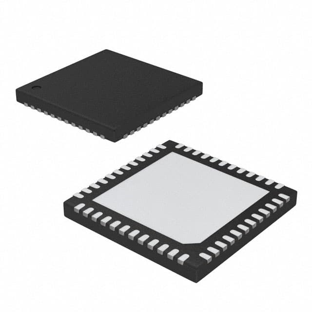
- Package: DCTM+ (Dual Flat No-Lead Package)
- Essence: Operational amplifier with high performance
- Packaging/Quantity: Tape and Reel, 2500 units per reel
Specifications and Parameters
- Supply Voltage Range: ±2.5V to ±18V
- Input Offset Voltage: 1mV (max)
- Gain Bandwidth Product: 100MHz (typ)
- Slew Rate: 400V/µs (typ)
- Input Bias Current: 10nA (max)
- Operating Temperature Range: -40°C to +85°C
Pin Configuration
The MAX4397DCTM+ has a total of 8 pins arranged as follows:
```
| | --| V- OUT |-- Pin 1 --| V+ IN- |-- Pin 2 --| NC IN+ |-- Pin 3 --| GND VCC |-- Pin 4 --| NC NC |-- Pin 5 --| NC NC |-- Pin 6 --| NC NC |-- Pin 7 --| NC NC |-- Pin 8 |___________| ```
Functional Characteristics
- High-speed amplification of input signals
- Low noise and distortion for accurate signal reproduction
- Wide supply voltage range for versatile applications
- Low input bias current for minimal loading effects
- Stable operation over a wide temperature range
Advantages and Disadvantages
Advantages: - High-speed performance - Low noise and distortion - Wide supply voltage range
Disadvantages: - Limited pin configuration options - No built-in protection features
Applicable Range of Products
The MAX4397DCTM+ is suitable for various applications, including: - Audio amplification - Instrumentation amplifiers - Signal conditioning circuits - Active filters - Data acquisition systems
Working Principles
The MAX4397DCTM+ operates as a voltage amplifier, taking an input signal and amplifying it with high speed and accuracy. It utilizes internal circuitry to provide low noise and distortion, ensuring faithful reproduction of the input signal.
Detailed Application Field Plans
- Audio Amplification: Use the MAX4397DCTM+ in audio systems to amplify weak signals from microphones or musical instruments.
- Instrumentation Amplifiers: Employ the MAX4397DCTM+ in precision measurement systems to amplify small sensor signals accurately.
- Signal Conditioning Circuits: Utilize the MAX4397DCTM+ to condition signals before further processing or analysis.
- Active Filters: Incorporate the MAX4397DCTM+ in active filter designs to shape frequency response characteristics.
- Data Acquisition Systems: Integrate the MAX4397DCTM+ into data acquisition modules for accurate signal acquisition and processing.
Detailed Alternative Models
Some alternative models to the MAX4397DCTM+ include: - AD8397 - LT6237 - OPA627
5 Common Technical Questions and Answers
Q: What is the maximum supply voltage for the MAX4397DCTM+? A: The maximum supply voltage is ±18V.
Q: Can the MAX4397DCTM+ operate at high temperatures? A: Yes, it can operate within the temperature range of -40°C to +85°C.
Q: Does the MAX4397DCTM+ have built-in protection features? A: No, it does not have built-in protection features.
Q: What is the typical gain bandwidth product of the MAX4397DCTM+? A: The typical gain bandwidth product is 100MHz.
Q: What is the input offset voltage of the MAX4397DCTM+? A: The input offset voltage is a maximum of 1mV.
This encyclopedia entry provides an overview of the MAX4397DCTM+, including its category, use, characteristics, package, specifications, pin configuration, functional characteristics, advantages and disadvantages, applicable range of products, working principles, detailed application field plans, alternative models, and common technical questions and answers.