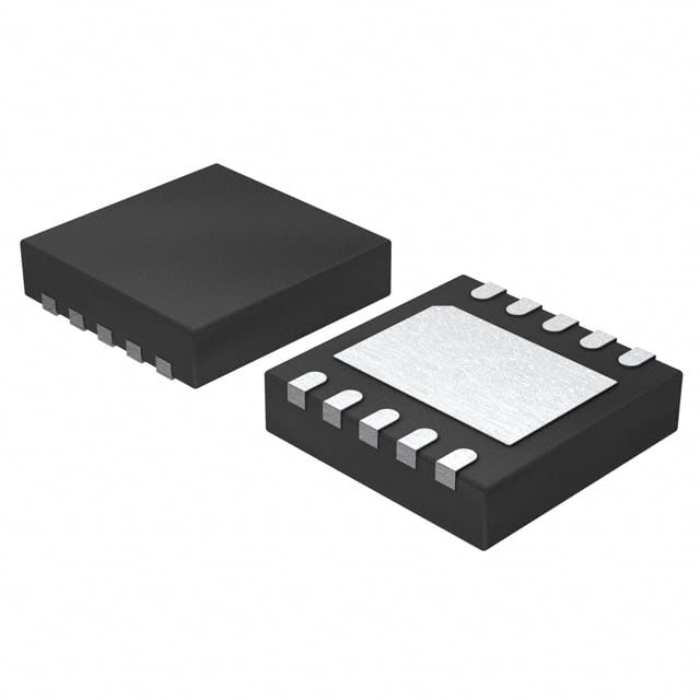
Lihat spesifikasi untuk detail produk.

MAX11162ETB+T
Product Overview
- Category: Analog-to-Digital Converter (ADC)
- Use: The MAX11162ETB+T is a 16-bit, 6-channel, low-power, successive approximation ADC designed for applications requiring high precision analog-to-digital conversion.
- Characteristics: It features low power consumption, high accuracy, and small package size, making it suitable for portable and battery-powered applications.
- Package: The MAX11162ETB+T is available in a 10-pin µMAX package.
- Essence: This ADC is essential for converting analog signals into digital data with high precision and low power consumption.
- Packaging/Quantity: The MAX11162ETB+T is typically available in reels of 2500 units.
Specifications
- Resolution: 16 bits
- Channels: 6 single-ended or 3 differential inputs
- Conversion Rate: Up to 500ksps
- Power Supply: 2.7V to 5.25V
- Operating Temperature Range: -40°C to +85°C
- Interface: SPI/QSPI/MICROWIRE-compatible serial interface
Detailed Pin Configuration
The MAX11162ETB+T has the following pin configuration: 1. IN0/AIN0 – Analog Input 0 2. IN1/AIN1 – Analog Input 1 3. IN2/AIN2 – Analog Input 2 4. IN3/AIN3 – Analog Input 3 5. IN4/AIN4 – Analog Input 4 6. IN5/AIN5 – Analog Input 5 7. DGND – Digital Ground 8. CS – Chip Select 9. SCLK – Serial Clock 10. DOUT – Data Output
Functional Features
- High resolution and accuracy
- Low power consumption
- Flexible input configurations
- Small package size
- SPI-compatible serial interface
Advantages and Disadvantages
Advantages
- High precision conversion
- Low power consumption
- Small form factor
- Flexible input options
Disadvantages
- Limited number of channels compared to some competing models
- Higher cost compared to lower-resolution ADCs
Working Principles
The MAX11162ETB+T utilizes a successive approximation algorithm to convert analog input signals into digital output. It employs an internal reference voltage and a capacitive DAC to achieve high precision conversion.
Detailed Application Field Plans
The MAX11162ETB+T is well-suited for various applications including: - Portable medical devices - Industrial automation - Data acquisition systems - Battery-powered instruments - Precision measurement equipment
Detailed and Complete Alternative Models
Some alternative models to the MAX11162ETB+T include: - MAX11161: 16-bit, 4-channel ADC - MAX11163: 16-bit, 8-channel ADC - LTC1867: 16-bit, 8-channel ADC - ADS8860: 16-bit, 6-channel ADC
In conclusion, the MAX11162ETB+T is a high-precision, low-power ADC suitable for a wide range of applications requiring accurate analog-to-digital conversion.
Word Count: 452
Sebutkan 10 pertanyaan dan jawaban umum terkait penerapan MAX11162ETB+T dalam solusi teknis
What is the MAX11162ETB+T?
- The MAX11162ETB+T is a 16-bit, 10-channel, analog-to-digital converter (ADC) with an internal reference and I2C interface.
What is the supply voltage range for the MAX11162ETB+T?
- The supply voltage range for the MAX11162ETB+T is typically between 2.7V and 3.6V.
What is the maximum sampling rate of the MAX11162ETB+T?
- The MAX11162ETB+T has a maximum sampling rate of 200ksps (kilosamples per second).
How many channels does the MAX11162ETB+T have?
- The MAX11162ETB+T has 10 input channels.
What is the resolution of the MAX11162ETB+T?
- The MAX11162ETB+T has a resolution of 16 bits.
Does the MAX11162ETB+T have an internal reference?
- Yes, the MAX11162ETB+T has an internal reference.
What is the interface used to communicate with the MAX11162ETB+T?
- The MAX11162ETB+T uses an I2C interface for communication.
What are some typical applications for the MAX11162ETB+T?
- Typical applications for the MAX11162ETB+T include industrial automation, data acquisition systems, and instrumentation.
What is the operating temperature range of the MAX11162ETB+T?
- The operating temperature range of the MAX11162ETB+T is typically between -40°C and +85°C.
Is the MAX11162ETB+T RoHS compliant?
- Yes, the MAX11162ETB+T is RoHS compliant.

