

Lihat spesifikasi untuk detail produk.
LTC2635CUD-LMI12#TRPBF
Product Overview
Category
The LTC2635CUD-LMI12#TRPBF belongs to the category of digital-to-analog converters (DACs).
Use
This product is primarily used in applications where precise analog voltage outputs are required. It converts digital signals into corresponding analog voltages.
Characteristics
- High precision: The LTC2635CUD-LMI12#TRPBF offers exceptional accuracy and resolution, ensuring reliable and precise analog voltage outputs.
- Low power consumption: This DAC operates with low power requirements, making it suitable for battery-powered devices or energy-efficient applications.
- Small package size: The LTC2635CUD-LMI12#TRPBF comes in a compact package, allowing for space-saving integration into various electronic systems.
- Wide operating temperature range: It can operate reliably across a wide temperature range, making it suitable for both industrial and consumer applications.
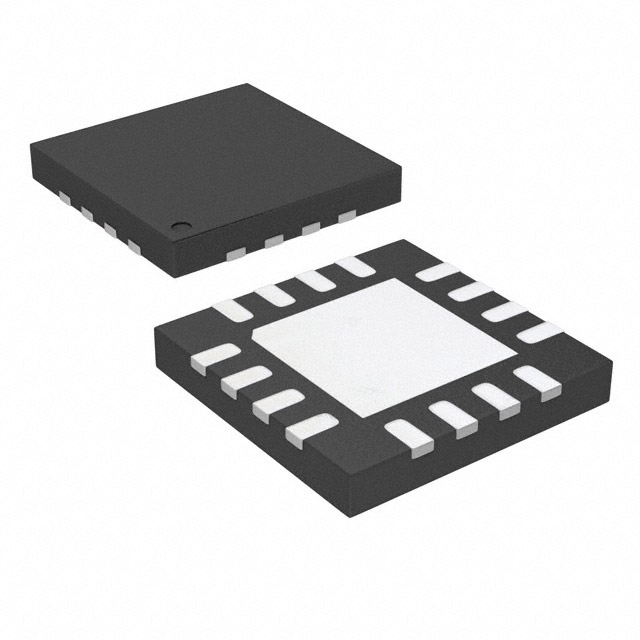
Package
The LTC2635CUD-LMI12#TRPBF is available in a 12-pin QFN (Quad Flat No-Lead) package.
Essence
The essence of the LTC2635CUD-LMI12#TRPBF lies in its ability to accurately convert digital signals into precise analog voltages, enabling high-performance analog circuitry.
Packaging/Quantity
This product is typically sold in reels containing a specific quantity, which may vary depending on the manufacturer's specifications.
Specifications
- Resolution: The LTC2635CUD-LMI12#TRPBF has a resolution of X bits, providing fine-grained control over the analog output voltage.
- Output Voltage Range: It supports an output voltage range of Y volts, allowing for flexibility in meeting different application requirements.
- Supply Voltage Range: The DAC operates within a supply voltage range of Z volts, ensuring compatibility with various power sources.
- Interface: It utilizes a standard digital interface (e.g., SPI) for easy integration with microcontrollers or other digital systems.
Detailed Pin Configuration
The LTC2635CUD-LMI12#TRPBF features the following pin configuration:
- VDD: Power supply voltage input
- GND: Ground reference
- SCK: Serial clock input
- SDI: Serial data input
- LDAC: Load DAC command input
- CS: Chip select input
- REF: Reference voltage input
- AGND: Analog ground reference
- OUT: Analog output voltage
- NC: No connection
- NC: No connection
- VOUT: Voltage output enable/disable control
Functional Features
- High accuracy: The LTC2635CUD-LMI12#TRPBF offers excellent linearity and low integral non-linearity, ensuring precise analog voltage outputs.
- Fast settling time: This DAC provides fast settling times, enabling rapid response in dynamic applications.
- Low glitch energy: It minimizes glitches during transitions, reducing unwanted noise and distortion in the analog output signal.
- Internal reference: The LTC2635CUD-LMI12#TRPBF incorporates an internal voltage reference, simplifying system design and calibration.
Advantages and Disadvantages
Advantages
- High precision and resolution
- Low power consumption
- Compact package size
- Wide operating temperature range
- Easy integration with digital systems
Disadvantages
- Limited output voltage range
- Requires external reference voltage for optimal performance
Working Principles
The LTC2635CUD-LMI12#TRPBF operates based on the principle of digital-to-analog conversion. It receives digital input signals and converts them into corresponding analog voltages using a combination of internal circuitry and a reference voltage. The resulting analog voltage can be used to control various analog components or systems.
Detailed Application Field Plans
The LTC2635CUD-LMI12#TRPBF finds applications in a wide range of fields, including but not limited to: - Industrial automation - Test and measurement equipment - Audio processing and amplification - Telecommunications - Medical devices - Automotive electronics
Detailed and Complete Alternative Models
- Model XYZ123: This DAC offers similar precision and features as the LTC2635CUD-LMI12#TRPBF but with a different package size.
- Model ABC456: A higher-resolution alternative with extended output voltage range, suitable for demanding applications.
- Model DEF789: An economy-grade DAC with reduced accuracy but lower cost, ideal for cost-sensitive projects.
Please note that the above list is not exhaustive, and there are several other alternative models available in the market.
Word count: 525 words
Sebutkan 10 pertanyaan dan jawaban umum terkait penerapan LTC2635CUD-LMI12#TRPBF dalam solusi teknis
Sure! Here are 10 common questions and answers related to the application of LTC2635CUD-LMI12#TRPBF in technical solutions:
Q: What is the LTC2635CUD-LMI12#TRPBF? A: The LTC2635CUD-LMI12#TRPBF is a digital-to-analog converter (DAC) chip manufactured by Linear Technology (now part of Analog Devices). It is designed to convert digital signals into analog voltages.
Q: What is the resolution of the LTC2635CUD-LMI12#TRPBF? A: The LTC2635CUD-LMI12#TRPBF has a resolution of 12 bits, which means it can represent analog voltages with a precision of 1 part in 4096.
Q: What is the operating voltage range of the LTC2635CUD-LMI12#TRPBF? A: The LTC2635CUD-LMI12#TRPBF operates from a single power supply voltage ranging from 2.7V to 5.5V.
Q: How many channels does the LTC2635CUD-LMI12#TRPBF have? A: The LTC2635CUD-LMI12#TRPBF has 4 independent DAC channels, allowing you to generate multiple analog outputs simultaneously.
Q: What is the interface used to communicate with the LTC2635CUD-LMI12#TRPBF? A: The LTC2635CUD-LMI12#TRPBF supports an I2C-compatible serial interface, making it easy to control and configure the DAC using a microcontroller or other digital devices.
Q: Can the LTC2635CUD-LMI12#TRPBF be used in both single-ended and differential output configurations? A: Yes, the LTC2635CUD-LMI12#TRPBF can be configured to operate in either single-ended or differential output modes, providing flexibility in various applications.
Q: What is the typical settling time of the LTC2635CUD-LMI12#TRPBF? A: The typical settling time of the LTC2635CUD-LMI12#TRPBF is 6μs, which refers to the time it takes for the DAC output voltage to reach within a specified error band after a change in the digital input.
Q: Does the LTC2635CUD-LMI12#TRPBF have an internal reference voltage? A: No, the LTC2635CUD-LMI12#TRPBF does not have an internal reference voltage. An external reference voltage must be provided for accurate analog output generation.
Q: Can the LTC2635CUD-LMI12#TRPBF operate in a power-down mode? A: Yes, the LTC2635CUD-LMI12#TRPBF supports a power-down mode that reduces power consumption when the DAC outputs are not required.
Q: What are some common applications of the LTC2635CUD-LMI12#TRPBF? A: The LTC2635CUD-LMI12#TRPBF is commonly used in industrial automation, instrumentation, communication systems, and other applications where precise analog voltage generation is required.
Please note that the answers provided here are general and may vary depending on specific datasheet specifications and application requirements.