

Lihat spesifikasi untuk detail produk.
LTC2630CSC6-LZ8#TRMPBF
Product Overview
Category
The LTC2630CSC6-LZ8#TRMPBF belongs to the category of digital-to-analog converters (DACs).
Use
This product is used to convert digital signals into analog voltage or current outputs.
Characteristics
- High precision: The LTC2630CSC6-LZ8#TRMPBF offers high-resolution and low integral nonlinearity, ensuring accurate conversion.
- Low power consumption: This DAC operates at a low power supply voltage, making it suitable for battery-powered applications.
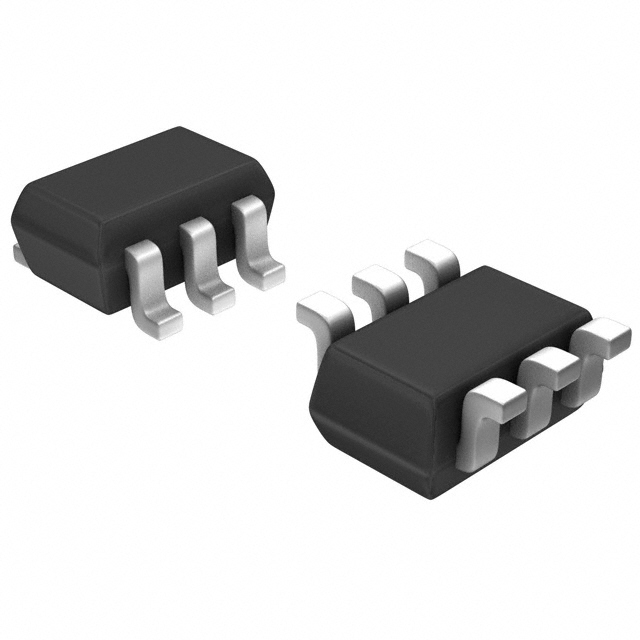
- Small package size: The LTC2630CSC6-LZ8#TRMPBF comes in a compact 6-pin SC70 package, saving board space.
- Wide temperature range: It can operate reliably over a wide temperature range, making it suitable for various environments.
Package and Quantity
The LTC2630CSC6-LZ8#TRMPBF is available in a SC70 package. It is typically sold in reels containing a specified quantity of units.
Specifications
- Resolution: 12 bits
- Number of channels: 1
- Supply voltage: 2.7V to 5.5V
- Output voltage range: 0V to Vref
- Operating temperature range: -40°C to +85°C
- Interface: SPI-compatible
Pin Configuration
The LTC2630CSC6-LZ8#TRMPBF has the following pin configuration:
```
| | --| VDD GND |-- Power supply pins --| SDA SCL |-- Serial data interface pins --| REF OUT |-- Reference voltage and analog output pins |___________| ```
Functional Features
- High accuracy: The LTC2630CSC6-LZ8#TRMPBF provides precise analog outputs with its high-resolution DAC.
- Easy interface: It utilizes a simple SPI-compatible interface for easy integration into various systems.
- Low power consumption: This DAC consumes minimal power, making it suitable for energy-efficient applications.
- Fast settling time: The LTC2630CSC6-LZ8#TRMPBF achieves fast settling times, enabling rapid response in dynamic applications.
Advantages and Disadvantages
Advantages
- High precision and accuracy
- Compact package size
- Wide temperature range operation
- Low power consumption
Disadvantages
- Limited number of channels (1 channel)
Working Principles
The LTC2630CSC6-LZ8#TRMPBF operates by converting digital input codes into corresponding analog voltages. It utilizes an internal reference voltage and a digital-to-analog conversion technique to achieve accurate and reliable analog outputs. The digital input codes are received through the serial data interface and converted into analog voltages, which can be used as control signals or inputs for various applications.
Detailed Application Field Plans
The LTC2630CSC6-LZ8#TRMPBF finds applications in various fields, including:
- Industrial automation: It can be used in process control systems, motor control, and instrumentation.
- Communications: This DAC is suitable for wireless communication systems, base stations, and network equipment.
- Consumer electronics: It can be utilized in audio systems, portable devices, and multimedia applications.
- Automotive: The LTC2630CSC6-LZ8#TRMPBF can be integrated into automotive electronics, such as infotainment systems and driver assistance modules.
Detailed and Complete Alternative Models
- LTC2630ACSC6-LZ8#TRMPBF: Similar to LTC2630CSC6-LZ8#TRMPBF but with extended temperature range (-40°C to +125°C).
- LTC2630BSC6-LZ8#TRMPBF: Similar to LTC2630CSC6-LZ8#TRMPBF but with 10-bit resolution.
- LTC2630DSC6-LZ8#TRMPBF: Similar to LTC2630CSC6-LZ8#TRMPBF but with 14-bit resolution.
These alternative models offer similar functionality and characteristics, providing options based on specific application requirements.
In conclusion, the LTC2630CSC6-LZ8#TRMPBF is a high-precision digital-to-analog converter with a compact package size and low power consumption. It offers accurate analog outputs and finds applications in various fields. Alternative models with different resolutions and temperature ranges are available to cater to specific needs.
Sebutkan 10 pertanyaan dan jawaban umum terkait penerapan LTC2630CSC6-LZ8#TRMPBF dalam solusi teknis
Sure! Here are 10 common questions and answers related to the application of LTC2630CSC6-LZ8#TRMPBF in technical solutions:
Q: What is LTC2630CSC6-LZ8#TRMPBF? A: LTC2630CSC6-LZ8#TRMPBF is a specific model of digital-to-analog converter (DAC) manufactured by Linear Technology.
Q: What is the purpose of LTC2630CSC6-LZ8#TRMPBF? A: The purpose of LTC2630CSC6-LZ8#TRMPBF is to convert digital signals into analog voltages, making it useful in various applications such as control systems, instrumentation, and communication devices.
Q: What is the resolution of LTC2630CSC6-LZ8#TRMPBF? A: LTC2630CSC6-LZ8#TRMPBF has a resolution of 12 bits, meaning it can represent analog voltages with 4096 discrete levels.
Q: What is the supply voltage range for LTC2630CSC6-LZ8#TRMPBF? A: The supply voltage range for LTC2630CSC6-LZ8#TRMPBF is typically between 2.7V and 5.5V.
Q: How many channels does LTC2630CSC6-LZ8#TRMPBF have? A: LTC2630CSC6-LZ8#TRMPBF is a dual-channel DAC, which means it has two independent output channels.
Q: What is the output voltage range of LTC2630CSC6-LZ8#TRMPBF? A: The output voltage range of LTC2630CSC6-LZ8#TRMPBF is 0V to Vref, where Vref is the reference voltage supplied to the DAC.
Q: What is the settling time of LTC2630CSC6-LZ8#TRMPBF? A: The settling time of LTC2630CSC6-LZ8#TRMPBF is typically around 10µs, which refers to the time it takes for the output voltage to reach within a specified error band after a change in the digital input.
Q: Can LTC2630CSC6-LZ8#TRMPBF operate in both unipolar and bipolar modes? A: Yes, LTC2630CSC6-LZ8#TRMPBF can be configured to operate in either unipolar mode (0V to Vref) or bipolar mode (-Vref/2 to +Vref/2).
Q: Does LTC2630CSC6-LZ8#TRMPBF have any built-in features for precision control? A: Yes, LTC2630CSC6-LZ8#TRMPBF includes an internal reference and a programmable gain amplifier (PGA), allowing for precise control over the output voltage range and resolution.
Q: What is the package type of LTC2630CSC6-LZ8#TRMPBF? A: LTC2630CSC6-LZ8#TRMPBF is available in a small 6-lead SC70 package, which is suitable for space-constrained applications.
Please note that the answers provided here are general and may vary depending on the specific datasheet and application requirements.