

Lihat spesifikasi untuk detail produk.
LTC2617IDE#TRPBF
Product Overview
Category
LTC2617IDE#TRPBF belongs to the category of digital-to-analog converters (DACs).
Use
This product is used to convert digital signals into analog voltages, making it suitable for various applications such as audio systems, instrumentation, and industrial control.
Characteristics
- High resolution: LTC2617IDE#TRPBF offers a resolution of up to 16 bits, ensuring accurate conversion of digital data.
- Low power consumption: This DAC operates at low power levels, making it energy-efficient.
- Small package size: The LTC2617IDE#TRPBF comes in a compact package, allowing for easy integration into space-constrained designs.
- Wide voltage range: It supports a wide supply voltage range, enabling compatibility with different power sources.
- Fast settling time: The DAC quickly settles to the desired output voltage, minimizing latency in signal processing.
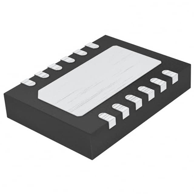
Package and Quantity
The LTC2617IDE#TRPBF is available in a 12-pin DFN (Dual Flat No-Lead) package. It is typically sold in reels, with a quantity of 2500 units per reel.
Specifications
- Resolution: Up to 16 bits
- Supply Voltage Range: 2.7V to 5.5V
- Output Voltage Range: 0V to VREF
- Operating Temperature Range: -40°C to 85°C
- Total Unadjusted Error: ±1 LSB (max)
- Integral Nonlinearity: ±1 LSB (max)
- Power Consumption: 0.6mW (typ)
Pin Configuration
The LTC2617IDE#TRPBF features a 12-pin DFN package with the following pin configuration:
- VDD: Power supply voltage input
- GND: Ground reference
- SDA: Serial data input
- SCL: Serial clock input
- A0: Address bit 0
- A1: Address bit 1
- A2: Address bit 2
- REF: Reference voltage input
- VOUT: Analog output voltage
- VREF: Reference voltage output
- AGND: Analog ground reference
- NC: No connection
Functional Features
- Multiple channels: The LTC2617IDE#TRPBF offers multiple independent DAC channels, allowing for simultaneous conversion of multiple digital signals.
- I2C interface: It utilizes the I2C communication protocol, enabling easy integration with microcontrollers and other digital devices.
- Software programmable: The DAC's output voltage can be programmed through software, providing flexibility in system design.
- Power-on reset: The device includes a power-on reset circuitry that ensures reliable operation upon power-up.
Advantages and Disadvantages
Advantages
- High resolution enables accurate analog signal generation.
- Low power consumption prolongs battery life in portable applications.
- Compact package size facilitates space-constrained designs.
- Wide voltage range enhances compatibility with various power sources.
- Fast settling time minimizes latency in signal processing.
Disadvantages
- Limited number of channels may restrict certain multi-channel applications.
- Higher cost compared to lower-resolution DACs.
Working Principles
The LTC2617IDE#TRPBF operates by receiving digital input data via the I2C interface. This digital data is then converted into an analog voltage using an internal digital-to-analog conversion algorithm. The resulting analog voltage is available at the VOUT pin, which can be connected to external circuitry for further processing or utilization.
Application Field Plans
The LTC2617IDE#TRPBF finds applications in various fields, including:
- Audio Systems: It can be used to generate high-quality analog audio signals in audio amplifiers, mixers, and digital musical instruments.
- Instrumentation: The DAC's accuracy and resolution make it suitable for precise control of test and measurement equipment.
- Industrial Control: It can be employed in industrial automation systems to generate analog control signals for motor drives, valves, and other actuators.
Alternative Models
- LTC2600: This series offers similar features but with lower resolution (10 bits).
- AD5628: Analog Devices' DAC provides 12-bit resolution and supports a wider supply voltage range.
- MAX5214: Maxim Integrated's DAC offers 14-bit resolution and includes an internal reference voltage source.
These alternative models provide different trade-offs in terms of resolution, voltage range, and additional features, allowing designers to choose the most suitable option for their specific application requirements.
Word count: 570 words
Sebutkan 10 pertanyaan dan jawaban umum terkait penerapan LTC2617IDE#TRPBF dalam solusi teknis
Sure! Here are 10 common questions and answers related to the application of LTC2617IDE#TRPBF:
Q: What is LTC2617IDE#TRPBF? A: LTC2617IDE#TRPBF is a specific model number for a digital-to-analog converter (DAC) chip manufactured by Linear Technology (now part of Analog Devices). It is used to convert digital signals into analog voltages.
Q: What is the operating voltage range of LTC2617IDE#TRPBF? A: The operating voltage range of LTC2617IDE#TRPBF is typically between 2.7V and 5.5V.
Q: How many channels does LTC2617IDE#TRPBF have? A: LTC2617IDE#TRPBF has 16 channels, which means it can simultaneously output 16 different analog voltages.
Q: What is the resolution of LTC2617IDE#TRPBF? A: LTC2617IDE#TRPBF has a resolution of 16 bits, which means it can represent 2^16 (65,536) different voltage levels.
Q: Can LTC2617IDE#TRPBF be controlled using an I2C interface? A: Yes, LTC2617IDE#TRPBF supports I2C communication protocol, making it easy to control and configure using microcontrollers or other devices with I2C capability.
Q: What is the maximum output voltage range of LTC2617IDE#TRPBF? A: The maximum output voltage range of LTC2617IDE#TRPBF is typically between 0V and Vref, where Vref is the reference voltage supplied to the chip.
Q: Does LTC2617IDE#TRPBF have built-in power-on reset circuitry? A: Yes, LTC2617IDE#TRPBF has a power-on reset circuit that ensures the DAC outputs are set to zero volts during power-up.
Q: Can LTC2617IDE#TRPBF operate in both unipolar and bipolar modes? A: Yes, LTC2617IDE#TRPBF can be configured to operate in either unipolar mode (0V to Vref) or bipolar mode (-Vref/2 to +Vref/2).
Q: What is the settling time of LTC2617IDE#TRPBF? A: The settling time of LTC2617IDE#TRPBF is typically around 10μs, which is the time it takes for the output voltage to reach within a specified error band after a change in the digital input.
Q: Can multiple LTC2617IDE#TRPBF chips be daisy-chained together? A: Yes, multiple LTC2617IDE#TRPBF chips can be daisy-chained together using the I2C interface, allowing for the control of multiple DAC channels with a single I2C bus.
Please note that the answers provided here are general and may vary depending on the specific application and configuration of LTC2617IDE#TRPBF. It is always recommended to refer to the datasheet and application notes for detailed information.