

Lihat spesifikasi untuk detail produk.
LTC2611CDD-1#TRPBF
Product Overview
Category
The LTC2611CDD-1#TRPBF belongs to the category of digital-to-analog converters (DACs).
Use
This product is primarily used in applications where a digital signal needs to be converted into an analog voltage or current. It finds extensive use in various electronic systems, including communication devices, industrial automation, audio equipment, and instrumentation.
Characteristics
- High precision: The LTC2611CDD-1#TRPBF offers exceptional accuracy in converting digital signals to analog outputs.
- Low power consumption: This DAC operates at low power levels, making it suitable for battery-powered devices.
- Fast settling time: The device provides rapid settling time, ensuring quick response in dynamic applications.
- Wide operating voltage range: The LTC2611CDD-1#TRPBF can operate within a wide voltage range, enhancing its versatility.
- Small package size: The product comes in a compact package, allowing for space-efficient integration into various systems.
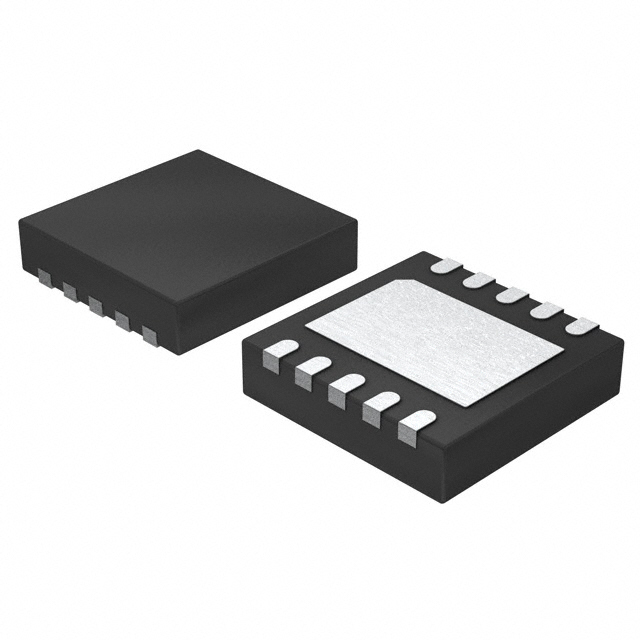
Package and Quantity
The LTC2611CDD-1#TRPBF is available in a 10-lead DFN (Dual Flat No-Lead) package. It is typically sold in reels, with a quantity of 2500 units per reel.
Specifications
- Resolution: 16 bits
- Output type: Voltage or current
- Supply voltage range: 2.7V to 5.5V
- Operating temperature range: -40°C to +85°C
- Integral nonlinearity (INL): ±1 LSB (max)
- Differential nonlinearity (DNL): ±1 LSB (max)
- Settling time: 4µs (typ)
Pin Configuration
The LTC2611CDD-1#TRPBF features a 10-lead DFN package with the following pin configuration:
- VDD: Supply voltage
- GND: Ground
- REF: Reference voltage input
- CS: Chip select input
- SCK: Serial clock input
- SDI: Serial data input
- LDAC: Load DAC input
- AGND: Analog ground
- OUT: Analog output
- NC: No connection
Functional Features
- High-resolution conversion: The LTC2611CDD-1#TRPBF offers 16-bit resolution, ensuring accurate and precise analog outputs.
- Serial interface: It utilizes a serial interface for easy integration into digital systems.
- Power-on reset: The device includes a power-on reset circuitry that ensures proper initialization upon power-up.
- Daisy-chain capability: Multiple LTC2611CDD-1#TRPBF devices can be daisy-chained together to simplify system design.
Advantages and Disadvantages
Advantages
- High precision and accuracy in digital-to-analog conversion.
- Low power consumption, making it suitable for portable and battery-powered applications.
- Fast settling time enables quick response in dynamic scenarios.
- Wide operating voltage range enhances versatility.
- Compact package size allows for space-efficient integration.
Disadvantages
- Limited output current capability compared to some other DACs.
- Higher cost compared to lower-resolution DACs.
Working Principles
The LTC2611CDD-1#TRPBF operates by converting a digital input signal into an analog output voltage or current. It utilizes an internal digital-to-analog conversion technique, which involves precise voltage references and a resistor ladder network. The digital input is processed and converted into an analog output with high accuracy and resolution.
Detailed Application Field Plans
The LTC2611CDD-1#TRPBF finds application in various fields, including: 1. Communication systems: Used for signal conditioning and modulation in wireless communication devices. 2. Industrial automation: Employed in control systems to generate precise analog signals for motor control, process control, and instrumentation. 3. Audio equipment: Utilized in audio amplifiers, mixers, and digital audio workstations for accurate sound reproduction. 4. Instrumentation: Integrated into test and measurement equipment to provide precise analog outputs for calibration and signal generation.
Detailed Alternative Models
- LTC2611IDD-1#PBF: Similar to LTC2611CDD-1#TRPBF but available in a 10-lead MSOP (Mini Small Outline Package).
- AD5621BKSZ-500RL7: A 12-bit DAC with similar characteristics and package options.
- MAX5216EUB+: A 16-bit DAC with additional features such as internal reference voltage and rail-to-rail output.
These alternative models offer similar functionality and can be considered based on specific application requirements.
In conclusion, the LTC2611CDD-1#TRPBF is a high-precision digital-to-analog converter used in various electronic systems. It offers
Sebutkan 10 pertanyaan dan jawaban umum terkait penerapan LTC2611CDD-1#TRPBF dalam solusi teknis
Sure! Here are 10 common questions and answers related to the application of LTC2611CDD-1#TRPBF in technical solutions:
Q1: What is LTC2611CDD-1#TRPBF? A1: LTC2611CDD-1#TRPBF is a specific model number for a digital-to-analog converter (DAC) chip manufactured by Linear Technology (now part of Analog Devices). It is used to convert digital signals into analog voltages.
Q2: What is the purpose of LTC2611CDD-1#TRPBF in technical solutions? A2: The LTC2611CDD-1#TRPBF DAC is commonly used in various technical solutions where precise analog voltage outputs are required, such as industrial control systems, instrumentation, audio equipment, and communication devices.
Q3: What is the resolution of LTC2611CDD-1#TRPBF? A3: LTC2611CDD-1#TRPBF has a resolution of 16 bits, which means it can provide 65,536 discrete voltage levels between its minimum and maximum output range.
Q4: What is the operating voltage range of LTC2611CDD-1#TRPBF? A4: LTC2611CDD-1#TRPBF operates with a supply voltage range of 2.7V to 5.5V.
Q5: How does LTC2611CDD-1#TRPBF communicate with a microcontroller or other digital devices? A5: LTC2611CDD-1#TRPBF uses a standard serial interface called I2C (Inter-Integrated Circuit) to communicate with microcontrollers or other digital devices.
Q6: Can LTC2611CDD-1#TRPBF handle multiple channels? A6: Yes, LTC2611CDD-1#TRPBF has two independent DAC channels, allowing it to generate two separate analog voltage outputs simultaneously.
Q7: What is the settling time of LTC2611CDD-1#TRPBF? A7: The settling time of LTC2611CDD-1#TRPBF is typically around 10µs, which refers to the time it takes for the output voltage to stabilize after a change in the digital input.
Q8: Does LTC2611CDD-1#TRPBF have any built-in reference voltage? A8: No, LTC2611CDD-1#TRPBF requires an external reference voltage source to determine its output voltage range.
Q9: Can LTC2611CDD-1#TRPBF operate in both unipolar and bipolar modes? A9: Yes, LTC2611CDD-1#TRPBF can be configured to operate in either unipolar mode (0V to Vref) or bipolar mode (-Vref/2 to +Vref/2), depending on the application requirements.
Q10: Is LTC2611CDD-1#TRPBF available in different package options? A10: Yes, LTC2611CDD-1#TRPBF is available in various package options, including DFN, MSOP, and SOIC, to accommodate different PCB layout and space constraints.
Please note that the answers provided here are general and may vary based on specific datasheet information and application requirements.