

Lihat spesifikasi untuk detail produk.
LFXP6E-4FN256C
Product Overview
Category
The LFXP6E-4FN256C belongs to the category of Field Programmable Gate Arrays (FPGAs).
Use
FPGAs are integrated circuits that can be programmed and reprogrammed to perform various digital functions. The LFXP6E-4FN256C is specifically designed for applications requiring high-performance and low-power consumption.
Characteristics
- High performance: The LFXP6E-4FN256C offers a high logic density and fast processing capabilities, making it suitable for complex digital designs.
- Low power consumption: This FPGA is optimized for power efficiency, allowing it to operate with minimal energy consumption.
- Flexible configuration: The device can be easily programmed and reconfigured to adapt to different application requirements.
Package
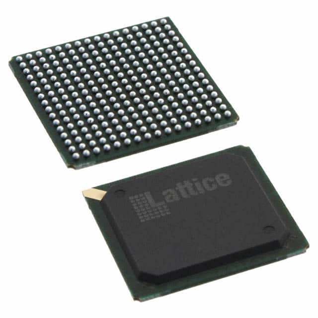
The LFXP6E-4FN256C comes in a 256-pin FineLine BGA package.
Essence
The essence of the LFXP6E-4FN256C lies in its ability to provide a versatile and efficient solution for digital circuit design and implementation.
Packaging/Quantity
The LFXP6E-4FN256C is typically sold individually or in reels, with the quantity depending on the supplier.
Specifications
- Logic Cells: 6,080
- Flip-Flops: 12,160
- Block RAM: 360 Kbits
- DSP Slices: 48
- Maximum Frequency: 400 MHz
- Operating Voltage: 1.2V
- I/O Standards: LVCMOS, LVTTL, SSTL, HSTL, LVDS, RSDS
Detailed Pin Configuration
The LFXP6E-4FN256C has a total of 256 pins. The pin configuration includes dedicated input/output pins, power supply pins, and configuration pins. For a detailed pinout diagram, please refer to the manufacturer's datasheet.
Functional Features
- High-speed performance: The LFXP6E-4FN256C offers fast processing capabilities, enabling efficient execution of complex digital algorithms.
- Low power consumption: With its optimized power efficiency, this FPGA minimizes energy consumption, making it suitable for battery-powered applications.
- Flexible I/O options: The device supports various I/O standards, allowing seamless integration with different external devices.
- Reconfigurability: The FPGA can be easily reprogrammed to adapt to changing application requirements, providing flexibility in design iterations.
Advantages and Disadvantages
Advantages
- High logic density enables complex digital designs.
- Low power consumption for energy-efficient operation.
- Versatile I/O options for seamless integration.
- Reconfigurable nature allows flexibility in design iterations.
Disadvantages
- Limited availability of alternative models with similar specifications.
- Steep learning curve for beginners due to the complexity of FPGA programming.
Working Principles
The LFXP6E-4FN256C operates based on the principles of configurable logic. It consists of an array of programmable logic blocks interconnected through configurable routing resources. These logic blocks can be programmed to implement desired digital functions using Hardware Description Languages (HDLs) such as VHDL or Verilog. Upon programming, the FPGA configures its internal connections to realize the desired functionality.
Detailed Application Field Plans
The LFXP6E-4FN256C finds applications in various fields, including:
- Communications: Used in wireless base stations, routers, and network switches for high-speed data processing.
- Industrial Automation: Employed in control systems, motor drives, and robotics for real-time control and signal processing.
- Aerospace and Defense: Utilized in radar systems, avionics, and secure communication systems for high-performance signal processing.
- Medical Devices: Integrated into medical imaging systems, patient monitoring devices, and diagnostic equipment for data processing and analysis.
Detailed and Complete Alternative Models
While the LFXP6E-4FN256C offers unique features, there are alternative models available in the market with similar specifications. Some notable alternatives include:
- Xilinx Artix-7 FPGA
- Intel Cyclone V FPGA
- Microsemi SmartFusion2 FPGA
These alternatives provide comparable performance and functionality, allowing designers to choose the most suitable option for their specific application requirements.
Word count: 536
Sebutkan 10 pertanyaan dan jawaban umum terkait penerapan LFXP6E-4FN256C dalam solusi teknis
Sure! Here are 10 common questions and answers related to the application of LFXP6E-4FN256C in technical solutions:
Q: What is the LFXP6E-4FN256C FPGA used for? A: The LFXP6E-4FN256C FPGA is commonly used for implementing digital logic circuits in various technical solutions.
Q: What is the maximum number of logic elements in the LFXP6E-4FN256C? A: The LFXP6E-4FN256C FPGA has a maximum of 6,000 logic elements.
Q: Can the LFXP6E-4FN256C be reprogrammed? A: Yes, the LFXP6E-4FN256C FPGA can be reprogrammed multiple times to implement different designs.
Q: What is the operating voltage range of the LFXP6E-4FN256C? A: The LFXP6E-4FN256C operates at a voltage range of 1.14V to 1.26V.
Q: Does the LFXP6E-4FN256C support high-speed interfaces like PCIe or Ethernet? A: Yes, the LFXP6E-4FN256C FPGA supports high-speed interfaces such as PCIe and Ethernet.
Q: What is the maximum clock frequency supported by the LFXP6E-4FN256C? A: The LFXP6E-4FN256C can operate at a maximum clock frequency of up to 400 MHz.
Q: Can the LFXP6E-4FN256C interface with external memory devices? A: Yes, the LFXP6E-4FN256C FPGA can interface with external memory devices like DDR3 or DDR4.
Q: Does the LFXP6E-4FN256C have built-in security features? A: Yes, the LFXP6E-4FN256C provides built-in security features like bitstream encryption and tamper detection.
Q: What development tools are available for programming the LFXP6E-4FN256C? A: The LFXP6E-4FN256C can be programmed using popular FPGA development tools like Xilinx Vivado or Intel Quartus Prime.
Q: Can the LFXP6E-4FN256C be used in industrial applications? A: Yes, the LFXP6E-4FN256C is suitable for various industrial applications due to its reliability and robustness.
Please note that the answers provided here are general and may vary depending on specific use cases and requirements.