

Lihat spesifikasi untuk detail produk.
LFXP2-17E-7FTN256C
Product Overview
Category
LFXP2-17E-7FTN256C belongs to the category of Field Programmable Gate Arrays (FPGAs).
Use
This product is primarily used in digital logic circuits for various applications such as telecommunications, automotive, industrial automation, and consumer electronics.
Characteristics
- High-performance FPGA with advanced features
- Low power consumption
- Flexible and reconfigurable design
- Large number of programmable logic cells
- High-speed data processing capabilities
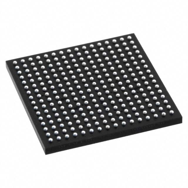
Package
LFXP2-17E-7FTN256C comes in a compact package that ensures easy integration into electronic systems. The package provides protection against environmental factors and facilitates efficient heat dissipation.
Essence
The essence of LFXP2-17E-7FTN256C lies in its ability to provide a customizable and versatile solution for complex digital circuit designs. It allows designers to implement their desired functionality by programming the FPGA.
Packaging/Quantity
LFXP2-17E-7FTN256C is typically packaged individually and is available in various quantities depending on the requirements of the user or project.
Specifications
- Logic Cells: 17,280
- Flip-Flops: 34,560
- Block RAM: 1,152 Kbits
- DSP Slices: 96
- I/O Pins: 256
- Operating Voltage: 1.2V
- Maximum Frequency: 400 MHz
- Configuration Memory: Flash-based
Detailed Pin Configuration
For a detailed pin configuration diagram of LFXP2-17E-7FTN256C, please refer to the manufacturer's datasheet.
Functional Features
- High-speed data processing capabilities enable real-time applications.
- Reconfigurable design allows for flexibility and adaptability in changing requirements.
- Large number of logic cells and flip-flops provide ample resources for complex designs.
- Integrated DSP slices enable efficient implementation of signal processing algorithms.
- Low power consumption makes it suitable for battery-powered devices.
Advantages
- Versatile and customizable solution for digital circuit designs.
- High-performance capabilities enable complex applications.
- Reconfigurable design allows for iterative development and quick prototyping.
- Low power consumption helps in reducing energy costs.
- Ample I/O pins facilitate easy interfacing with other components.
Disadvantages
- Steep learning curve for beginners due to the complexity of FPGA programming.
- Higher cost compared to traditional fixed-function integrated circuits.
- Limited availability of alternative models from different manufacturers.
Working Principles
LFXP2-17E-7FTN256C operates based on the principles of field-programmable gate arrays. It consists of a large number of configurable logic blocks interconnected through programmable routing resources. The functionality of the FPGA is determined by the configuration data stored in its memory. During operation, the FPGA can be reprogrammed to implement different logic functions, allowing for flexibility and adaptability.
Detailed Application Field Plans
LFXP2-17E-7FTN256C finds applications in various fields, including:
- Telecommunications: Used in base stations, network switches, and routers for high-speed data processing and protocol handling.
- Automotive: Employed in advanced driver-assistance systems (ADAS) for real-time image processing and sensor fusion.
- Industrial Automation: Utilized in programmable logic controllers (PLCs) for controlling and monitoring industrial processes.
- Consumer Electronics: Integrated into smart TVs, gaming consoles, and multimedia devices for enhanced performance and functionality.
Detailed and Complete Alternative Models
While LFXP2-17E-7FTN256C is a highly capable FPGA, there are alternative models available from different manufacturers that offer similar functionality. Some notable alternatives include:
- Xilinx Virtex UltraScale+ series
- Intel (formerly Altera) Stratix 10 series
- Microsemi (now Microchip) PolarFire series
These alternative models provide a range of options with varying performance, capacity, and features to suit different application requirements.
Word count: 517
Sebutkan 10 pertanyaan dan jawaban umum terkait penerapan LFXP2-17E-7FTN256C dalam solusi teknis
Sure! Here are 10 common questions and answers related to the application of LFXP2-17E-7FTN256C in technical solutions:
Q: What is the LFXP2-17E-7FTN256C? A: The LFXP2-17E-7FTN256C is a field-programmable gate array (FPGA) manufactured by Lattice Semiconductor.
Q: What are the key features of the LFXP2-17E-7FTN256C? A: The key features include 17,280 Look-Up Tables (LUTs), 256 I/O pins, 7ns maximum delay, and 256Kbits embedded block RAM.
Q: What are some typical applications for the LFXP2-17E-7FTN256C? A: The LFXP2-17E-7FTN256C is commonly used in applications such as industrial automation, telecommunications, automotive electronics, and medical devices.
Q: How can I program the LFXP2-17E-7FTN256C? A: The LFXP2-17E-7FTN256C can be programmed using Lattice Diamond or Lattice Radiant software tools provided by Lattice Semiconductor.
Q: Can I use the LFXP2-17E-7FTN256C for high-speed data processing? A: Yes, the LFXP2-17E-7FTN256C has a maximum delay of 7ns, making it suitable for high-speed data processing applications.
Q: Does the LFXP2-17E-7FTN256C support external memory interfaces? A: Yes, the LFXP2-17E-7FTN256C supports various external memory interfaces such as DDR3, DDR4, and LPDDR.
Q: Can I interface the LFXP2-17E-7FTN256C with other microcontrollers or processors? A: Yes, the LFXP2-17E-7FTN256C can be interfaced with other microcontrollers or processors using standard communication protocols like SPI, I2C, or UART.
Q: What is the power supply requirement for the LFXP2-17E-7FTN256C? A: The LFXP2-17E-7FTN256C requires a 1.2V core voltage and a 3.3V I/O voltage for proper operation.
Q: Is the LFXP2-17E-7FTN256C suitable for low-power applications? A: Yes, the LFXP2-17E-7FTN256C has power-saving features such as dynamic power management and clock gating, making it suitable for low-power applications.
Q: Where can I find additional technical documentation and support for the LFXP2-17E-7FTN256C? A: You can find additional technical documentation, application notes, and support resources on the official website of Lattice Semiconductor or by contacting their customer support team.