

Lihat spesifikasi untuk detail produk.
LFE2-50E-5FN672C
Product Overview
Category
The LFE2-50E-5FN672C belongs to the category of Field Programmable Gate Arrays (FPGAs).
Use
FPGAs are integrated circuits that can be programmed and reprogrammed to perform various digital functions. The LFE2-50E-5FN672C is specifically designed for applications requiring high-performance and low-power consumption.
Characteristics
- High-performance FPGA with low-power consumption
- Programmable and reprogrammable
- Suitable for a wide range of applications
- Compact package size
- Advanced features for efficient design implementation
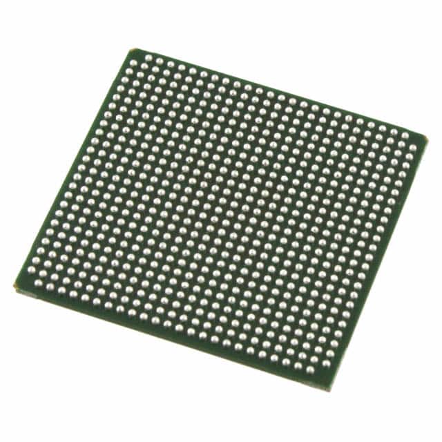
Package
The LFE2-50E-5FN672C comes in a compact package, which ensures easy integration into electronic systems. The package provides protection against environmental factors and facilitates efficient heat dissipation.
Essence
The essence of the LFE2-50E-5FN672C lies in its ability to provide flexible and customizable digital functionality. It allows designers to implement complex logic circuits and algorithms in a single chip, eliminating the need for multiple discrete components.
Packaging/Quantity
The LFE2-50E-5FN672C is typically packaged individually and is available in various quantities depending on the requirements of the application.
Specifications
- FPGA Family: Lattice ECP2M
- Logic Elements: 50,000
- Number of I/O Pins: 672
- Operating Voltage: 1.2V
- Maximum Frequency: 400 MHz
- Embedded Memory: Up to 4.8 Mbits
- Configuration Memory: Flash-based
Detailed Pin Configuration
The LFE2-50E-5FN672C has 672 I/O pins, each serving a specific purpose in the system. The pin configuration varies depending on the application requirements and the designer's implementation.
Functional Features
- High-performance digital signal processing capabilities
- Flexible and customizable logic functions
- Support for various communication protocols
- Efficient power management features
- On-chip memory for data storage and retrieval
- Built-in security features for protecting intellectual property
Advantages and Disadvantages
Advantages
- Versatile and adaptable to a wide range of applications
- High-performance capabilities with low-power consumption
- Simplifies system design by integrating multiple functions into a single chip
- Reduces time-to-market by allowing rapid prototyping and iteration
- Cost-effective compared to custom ASIC designs
Disadvantages
- Limited scalability compared to dedicated hardware solutions
- Higher initial development cost compared to off-the-shelf components
- Requires specialized knowledge and expertise for efficient programming and utilization
Working Principles
The LFE2-50E-5FN672C operates based on the principles of reconfigurable computing. It consists of an array of programmable logic elements interconnected through configurable routing resources. The device can be programmed using Hardware Description Languages (HDL) such as VHDL or Verilog, which define the desired functionality and interconnections within the FPGA.
During operation, the FPGA executes the programmed logic circuits, enabling the desired digital functions. The reprogrammability of the LFE2-50E-5FN672C allows for iterative design improvements and modifications without requiring hardware changes.
Detailed Application Field Plans
The LFE2-50E-5FN672C finds applications in various fields, including:
- Communications: Used in wireless base stations, routers, and network switches for high-speed data processing and protocol handling.
- Industrial Automation: Enables real-time control and monitoring in industrial systems, including robotics, process automation, and machine vision.
- Automotive: Utilized in advanced driver assistance systems (ADAS), infotainment systems, and engine control units (ECUs) for enhanced performance and functionality.
- Aerospace and Defense: Used in radar systems, avionics, and secure communication systems for high-reliability and mission-critical applications.
Detailed and Complete Alternative Models
- Xilinx Virtex-7 XC7VX485T: Offers similar performance and features with a larger logic capacity.
- Intel Cyclone V EP5CE115F23I7N: Provides a cost-effective alternative with lower power consumption.
- Microsemi SmartFusion2 M2S010: Combines FPGA capabilities with integrated ARM Cortex-M3 processor for embedded system applications.
These alternative models offer different trade-offs in terms of performance, power consumption, and price, allowing designers to choose the most suitable option for their specific requirements.
Word count: 570 words
Sebutkan 10 pertanyaan dan jawaban umum terkait penerapan LFE2-50E-5FN672C dalam solusi teknis
Sure! Here are 10 common questions and answers related to the application of LFE2-50E-5FN672C in technical solutions:
Q: What is LFE2-50E-5FN672C? A: LFE2-50E-5FN672C is a specific model of Field-Programmable Gate Array (FPGA) manufactured by Lattice Semiconductor.
Q: What are the key features of LFE2-50E-5FN672C? A: Some key features of LFE2-50E-5FN672C include 50,000 Look-Up Tables (LUTs), 672-pin Fine-Pitch Ball Grid Array (FBGA) package, and support for various I/O standards.
Q: What are the typical applications of LFE2-50E-5FN672C? A: LFE2-50E-5FN672C can be used in a wide range of applications such as industrial automation, telecommunications, automotive electronics, and medical devices.
Q: How can LFE2-50E-5FN672C be programmed? A: LFE2-50E-5FN672C can be programmed using hardware description languages (HDL) like VHDL or Verilog, or through graphical programming tools provided by Lattice Semiconductor.
Q: What is the power supply requirement for LFE2-50E-5FN672C? A: LFE2-50E-5FN672C requires a single power supply voltage of 1.2V.
Q: Can LFE2-50E-5FN672C interface with other components or devices? A: Yes, LFE2-50E-5FN672C supports various I/O standards such as LVCMOS, LVTTL, and SSTL, allowing it to interface with other components or devices.
Q: Is LFE2-50E-5FN672C suitable for high-speed applications? A: Yes, LFE2-50E-5FN672C is designed to support high-speed applications with its advanced architecture and optimized routing resources.
Q: Can LFE2-50E-5FN672C be reprogrammed after deployment? A: Yes, LFE2-50E-5FN672C is a reprogrammable FPGA, which means it can be reconfigured even after it has been deployed in a system.
Q: Are there any development tools available for LFE2-50E-5FN672C? A: Yes, Lattice Semiconductor provides development tools like Lattice Diamond software suite, which includes design entry, synthesis, simulation, and programming tools.
Q: Where can I find more information about LFE2-50E-5FN672C? A: You can find more detailed information about LFE2-50E-5FN672C on the official website of Lattice Semiconductor or by referring to the datasheet and application notes provided by the manufacturer.