

Lihat spesifikasi untuk detail produk.
LCMXO3L-4300C-5BG400I
Product Overview
Category
The LCMXO3L-4300C-5BG400I belongs to the category of Field Programmable Gate Arrays (FPGAs).
Use
FPGAs are integrated circuits that can be programmed and reprogrammed to perform various digital functions. The LCMXO3L-4300C-5BG400I is specifically designed for applications requiring high-performance and low-power consumption.
Characteristics
- High performance: The LCMXO3L-4300C-5BG400I offers a high logic density and fast processing capabilities, making it suitable for complex digital designs.
- Low power consumption: This FPGA is optimized for low power operation, making it ideal for battery-powered devices or energy-efficient applications.
- Small package size: The LCMXO3L-4300C-5BG400I comes in a compact package, allowing for space-saving integration into electronic systems.
- Versatile I/O options: It provides a wide range of input/output options, enabling connectivity with other components and peripherals.
- Robust packaging: The LCMXO3L-4300C-5BG400I is packaged in a durable and reliable manner, ensuring protection during handling and installation.
Packaging/Quantity
The LCMXO3L-4300C-5BG400I is typically available in a surface-mount package. The exact quantity per package may vary depending on the supplier.
Specifications
- Logic elements: 4,300
- Look-up tables (LUTs): 2,150
- Flip-flops: 4,300
- Block RAM: 112 Kbits
- Maximum frequency: 250 MHz
- I/O pins: 400
- Operating voltage: 1.2V
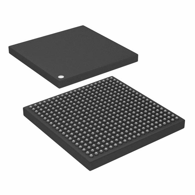
- Package type: BGA (Ball Grid Array)
- Package size: 17mm x 17mm
Detailed Pin Configuration
The LCMXO3L-4300C-5BG400I has a total of 400 I/O pins, which are configurable for various purposes. The pin configuration may vary depending on the specific application requirements. Please refer to the manufacturer's datasheet for detailed pin assignments.
Functional Features
- Programmability: The LCMXO3L-4300C-5BG400I can be programmed using hardware description languages (HDL) or graphical design tools, allowing for flexible and customizable digital circuit designs.
- Reconfigurability: It supports dynamic reconfiguration, enabling on-the-fly changes to the FPGA's functionality without the need for hardware modifications.
- Embedded memory: The built-in block RAM provides dedicated memory resources for data storage and processing within the FPGA.
- Clock management: The LCMXO3L-4300C-5BG400I includes clock management features, such as PLLs (Phase-Locked Loops), to generate and distribute precise clock signals throughout the system.
- High-speed interfaces: It supports various high-speed serial communication protocols, such as PCIe (Peripheral Component Interconnect Express) and Ethernet, facilitating connectivity with external devices.
Advantages and Disadvantages
Advantages
- High performance and low power consumption make it suitable for demanding applications.
- Compact package size allows for space-efficient integration into electronic systems.
- Versatile I/O options enable connectivity with a wide range of components and peripherals.
- Reconfigurability offers flexibility for future design changes or updates.
- Built-in memory resources provide efficient data storage and processing capabilities.
Disadvantages
- Limited logic elements compared to larger FPGAs, which may restrict the complexity of designs that can be implemented.
- Higher cost compared to other programmable logic devices, such as CPLDs (Complex Programmable Logic Devices).
- Steeper learning curve for programming and utilizing the full potential of FPGAs compared to traditional microcontrollers.
Working Principles
The LCMXO3L-4300C-5BG400I operates based on the principles of configurable logic. It consists of an array of programmable logic elements, interconnected by configurable routing resources. These logic elements can be programmed to implement various digital functions, such as arithmetic operations, data processing, and control logic. The configuration data is stored in internal memory cells and can be modified using programming tools. During operation, the FPGA dynamically routes signals through the configured logic elements to perform the desired functionality.
Detailed Application Field Plans
The LCMXO3L-4300C-5BG400I finds applications in a wide range of fields, including:
- Communications: Used in networking equipment, routers, and switches for high-speed data processing and protocol handling.
- Industrial automation: Employed in control systems, motor drives, and robotics for real-time control and signal processing.
- Automotive electronics: Integrated into automotive systems
Sebutkan 10 pertanyaan dan jawaban umum terkait penerapan LCMXO3L-4300C-5BG400I dalam solusi teknis
Sure! Here are 10 common questions and answers related to the application of LCMXO3L-4300C-5BG400I in technical solutions:
Q: What is the LCMXO3L-4300C-5BG400I? A: The LCMXO3L-4300C-5BG400I is a low-cost, low-power FPGA (Field-Programmable Gate Array) device manufactured by Lattice Semiconductor.
Q: What are the key features of the LCMXO3L-4300C-5BG400I? A: The key features include 4300 LUTs (Look-Up Tables), 64 I/O pins, 4Kbits of embedded memory, and support for various I/O standards.
Q: What are some typical applications of the LCMXO3L-4300C-5BG400I? A: The LCMXO3L-4300C-5BG400I is commonly used in applications such as industrial automation, consumer electronics, IoT devices, and automotive systems.
Q: How can I program the LCMXO3L-4300C-5BG400I? A: The LCMXO3L-4300C-5BG400I can be programmed using Lattice Diamond or Lattice Radiant software tools, which support various programming languages like VHDL and Verilog.
Q: What voltage levels does the LCMXO3L-4300C-5BG400I support? A: The LCMXO3L-4300C-5BG400I supports both 3.3V and 1.2V voltage levels, making it compatible with a wide range of digital systems.
Q: Can I use the LCMXO3L-4300C-5BG400I in battery-powered devices? A: Yes, the LCMXO3L-4300C-5BG400I is designed to be low-power, making it suitable for battery-powered applications where power consumption is a concern.
Q: Does the LCMXO3L-4300C-5BG400I have any built-in communication interfaces? A: Yes, the LCMXO3L-4300C-5BG400I supports various communication interfaces such as SPI, I2C, UART, and GPIOs, allowing easy integration with other devices.
Q: Can I reprogram the LCMXO3L-4300C-5BG400I multiple times? A: Yes, the LCMXO3L-4300C-5BG400I is a reprogrammable FPGA, which means you can program it multiple times to implement different functionalities.
Q: Are there any development boards available for the LCMXO3L-4300C-5BG400I? A: Yes, Lattice Semiconductor provides development boards like the LCMXO3L-EVN, which allow easy prototyping and evaluation of the LCMXO3L-4300C-5BG400I.
Q: Where can I find technical documentation and support for the LCMXO3L-4300C-5BG400I? A: You can find technical documentation, datasheets, application notes, and support resources on the official Lattice Semiconductor website or by contacting their customer support team.
Please note that the answers provided here are general and may vary depending on specific requirements and use cases.