

Lihat spesifikasi untuk detail produk.
LCMXO256E-3M100C
Product Overview
Category
The LCMXO256E-3M100C belongs to the category of Field Programmable Gate Arrays (FPGAs).
Use
FPGAs are integrated circuits that can be programmed and reprogrammed to perform various digital functions. The LCMXO256E-3M100C is specifically designed for applications requiring high-performance and low-power consumption.
Characteristics
- High-performance FPGA with low power consumption
- Programmable and reprogrammable
- Suitable for a wide range of applications
- Compact package size
- Offers flexibility in design and implementation
Package
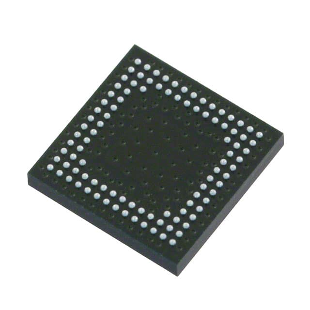
The LCMXO256E-3M100C comes in a compact 100-pin Quad Flat No-Lead (QFN) package.
Essence
The essence of the LCMXO256E-3M100C lies in its ability to provide a customizable and flexible solution for digital circuit design and implementation.
Packaging/Quantity
The LCMXO256E-3M100C is typically packaged individually and is available in various quantities depending on the manufacturer or distributor.
Specifications
- FPGA Family: Lattice XO2
- Logic Cells: 256
- Speed Grade: -3
- Package Type: QFN
- Package Pins: 100
- Operating Voltage: 1.2V
- Operating Temperature Range: -40°C to +85°C
- Maximum Frequency: 100 MHz
- I/O Standards: LVCMOS, LVTTL, SSTL, HSTL, LVDS, RSDS
Detailed Pin Configuration
The LCMXO256E-3M100C has a total of 100 pins. The pin configuration varies based on the specific application requirements and design considerations. Please refer to the datasheet or user manual for the detailed pin configuration of the LCMXO256E-3M100C.
Functional Features
- High-performance digital circuit implementation
- Low power consumption
- Flexible and customizable design options
- Support for various I/O standards
- On-chip memory resources
- Built-in security features
- Easy integration with other components/systems
Advantages and Disadvantages
Advantages
- Versatile and flexible solution for digital circuit design
- High-performance capabilities
- Low power consumption
- Compact package size
- Wide range of supported I/O standards
- On-chip memory resources for efficient data processing
Disadvantages
- Limited logic cell count compared to higher-end FPGAs
- May require additional external components for specific applications
- Steeper learning curve for programming and utilization compared to traditional ASICs
Working Principles
The LCMXO256E-3M100C operates based on the principles of reconfigurable logic. It consists of programmable logic blocks, interconnect resources, and I/O elements. The programmable logic blocks can be configured to implement various digital functions, while the interconnect resources allow for the routing of signals between different blocks. The I/O elements provide interfaces for communication with external devices.
The FPGA is programmed using a Hardware Description Language (HDL) such as VHDL or Verilog. The desired functionality is described in the HDL code, which is then synthesized and mapped onto the FPGA. Once programmed, the FPGA can perform the specified digital functions.
Detailed Application Field Plans
The LCMXO256E-3M100C finds applications in various fields, including but not limited to:
- Communications: Used in wireless base stations, network routers, and switches for signal processing and protocol handling.
- Industrial Automation: Employed in control systems, robotics, and machine vision applications for real-time data processing and control.
- Automotive: Integrated into automotive electronics for functions like engine control, infotainment systems, and driver assistance systems.
- Aerospace and Defense: Utilized in radar systems, avionics, and military communication systems for high-performance signal processing and encryption.
- Consumer Electronics: Incorporated into smart TVs, gaming consoles, and wearable devices for multimedia processing and user interface control.
Detailed and Complete Alternative Models
- Xilinx Spartan-6 XC6SLX9 FPGA
- Altera Cyclone IV EP4CE6E22C8N FPGA
- Microsemi IGLOO2 M2GL090 FPGA
- Intel MAX 10 10M08SAE144C8G FPGA
- QuickLogic EOS S3 LP FPGA
These alternative models offer similar functionalities and can be considered as alternatives to the LCMXO256E-3M100C based on specific application requirements and design considerations.
Word count: 570 words
Sebutkan 10 pertanyaan dan jawaban umum terkait penerapan LCMXO256E-3M100C dalam solusi teknis
Sure! Here are 10 common questions and answers related to the application of LCMXO256E-3M100C in technical solutions:
Q: What is the LCMXO256E-3M100C? A: The LCMXO256E-3M100C is a low-cost, low-power FPGA (Field-Programmable Gate Array) device manufactured by Lattice Semiconductor.
Q: What are the key features of the LCMXO256E-3M100C? A: The key features include 256 LUTs (Look-Up Tables), 4,000 logic cells, 8 multipliers, 32Kbits of embedded memory, and support for various I/O standards.
Q: What are some typical applications of the LCMXO256E-3M100C? A: The LCMXO256E-3M100C is commonly used in applications such as industrial control systems, consumer electronics, automotive electronics, and IoT devices.
Q: How can I program the LCMXO256E-3M100C? A: The LCMXO256E-3M100C can be programmed using Lattice Diamond or Lattice Radiant software tools, which provide a graphical interface for designing and programming the FPGA.
Q: What voltage levels does the LCMXO256E-3M100C support? A: The LCMXO256E-3M100C supports both 3.3V and 1.2V voltage levels, making it compatible with a wide range of digital systems.
Q: Can I use the LCMXO256E-3M100C for high-speed applications? A: While the LCMXO256E-3M100C is not specifically designed for high-speed applications, it can still handle moderate-speed designs depending on the specific requirements.
Q: Does the LCMXO256E-3M100C have any built-in communication interfaces? A: Yes, the LCMXO256E-3M100C supports various communication interfaces such as SPI, I2C, UART, and GPIOs, allowing easy integration with other devices.
Q: Can I use the LCMXO256E-3M100C in battery-powered applications? A: Yes, the LCMXO256E-3M100C is known for its low power consumption, making it suitable for battery-powered applications where power efficiency is crucial.
Q: Are there any development boards available for the LCMXO256E-3M100C? A: Yes, Lattice Semiconductor offers development boards like the LCMXO256E-B-EVN, which provide a convenient platform for prototyping and testing designs.
Q: Where can I find more technical information about the LCMXO256E-3M100C? A: You can find detailed technical documentation, datasheets, application notes, and reference designs on the official Lattice Semiconductor website or by contacting their support team.
Please note that the answers provided here are general and may vary based on specific design requirements and application scenarios.