

Lihat spesifikasi untuk detail produk.
LC4512V-10FTN256I
Product Overview
Category: Integrated Circuit (IC)
Use: The LC4512V-10FTN256I is a programmable logic device (PLD) that belongs to the family of Complex Programmable Logic Devices (CPLDs). It is designed for digital logic applications and offers high-performance, low-power consumption, and flexibility in design.
Characteristics: - High-density programmable logic device - Low power consumption - Flexible design options - Fast performance
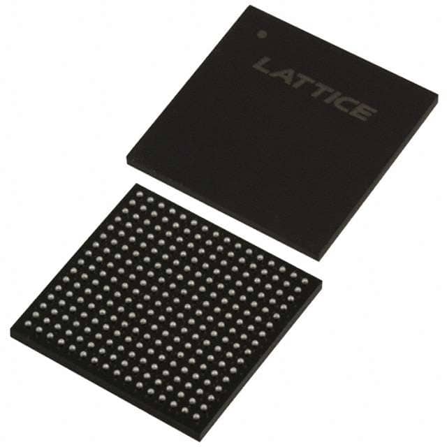
Package: The LC4512V-10FTN256I is available in a 256-pin Fine-Pitch Ball Grid Array (FBGA) package. This package provides a compact form factor and excellent thermal characteristics.
Essence: The essence of the LC4512V-10FTN256I lies in its ability to implement complex digital logic functions in a single integrated circuit. It offers designers the flexibility to create custom logic designs tailored to their specific requirements.
Packaging/Quantity: The LC4512V-10FTN256I is typically sold individually in anti-static packaging to ensure proper handling and protection during transportation. The exact quantity may vary depending on the supplier.
Specifications
- Device Type: Complex Programmable Logic Device (CPLD)
- Family: LC4000V
- Number of Macrocells: 512
- Operating Voltage: 3.3V
- Speed Grade: -10
- Package Type: 256-pin FBGA
- Temperature Range: Commercial (0°C to 70°C)
- I/O Pins: 192
- JTAG Boundary Scan Support: Yes
Detailed Pin Configuration
The LC4512V-10FTN256I has a total of 256 pins. Here is a brief overview of the pin configuration:
- VCCIO: Power supply voltage for I/O pins
- GND: Ground reference
- VCCINT: Power supply voltage for internal circuitry
- JTAGTMS, JTAGTCK, JTAGTDI, JTAGTDO: JTAG interface pins for boundary scan support
- I/O Pins: Bidirectional input/output pins for connecting external devices
- Clock Inputs: Pins for providing clock signals to the device
- Configuration Pins: Pins for programming and configuring the device
For a detailed pinout diagram and further information, refer to the LC4512V-10FTN256I datasheet.
Functional Features
The LC4512V-10FTN256I offers several functional features that make it suitable for a wide range of digital logic applications:
- High-Density Logic: With 512 macrocells, the device can implement complex logic functions in a compact form factor.
- Flexible I/O Options: The 192 bidirectional I/O pins provide versatility in connecting external devices.
- Fast Performance: The CPLD operates at high speeds, enabling efficient execution of digital logic operations.
- Low Power Consumption: The device is designed to minimize power consumption, making it suitable for battery-powered applications.
- JTAG Boundary Scan Support: The built-in JTAG interface allows for easy testing and debugging of the device during development.
Advantages and Disadvantages
Advantages: - High-density programmable logic device - Flexible design options - Fast performance - Low power consumption - JTAG boundary scan support for easy testing and debugging
Disadvantages: - Limited number of I/O pins compared to some other CPLDs - Higher cost compared to simpler programmable logic devices
Working Principles
The LC4512V-10FTN256I utilizes a combination of look-up tables (LUTs), flip-flops, and interconnect resources to implement digital logic functions. The device is programmed using Hardware Description Language (HDL) or a graphical design tool, which generates a configuration file. This file is then loaded into the CPLD to define the desired logic functionality.
During operation, the inputs to the CPLD are processed through the LUTs, which perform the required logic operations. The output of the LUTs is stored in flip-flops, providing sequential logic capabilities. The interconnect resources allow for routing signals between different macrocells and I/O pins.
Detailed Application Field Plans
The LC4512V-10FTN256I can be applied in various fields, including:
- Communications: Used in networking equipment, routers, and switches for implementing custom logic functions.
- Industrial Control Systems: Employed in programmable logic controllers (PLCs) for automation and control applications.
- Consumer Electronics: Integrated into smart home devices, gaming consoles, and multimedia systems for customized functionality.
- Automotive: Utilized in automotive electronics for implementing specialized features in vehicle control systems.
- Medical Devices: Incorporated into medical equipment for custom signal processing and control functions.
Detailed
Sebutkan 10 pertanyaan dan jawaban umum terkait penerapan LC4512V-10FTN256I dalam solusi teknis
Sure! Here are 10 common questions and answers related to the application of LC4512V-10FTN256I in technical solutions:
1. What is LC4512V-10FTN256I? - LC4512V-10FTN256I is a specific model of Field-Programmable Gate Array (FPGA) manufactured by Lattice Semiconductor.
2. What are the key features of LC4512V-10FTN256I? - Some key features of LC4512V-10FTN256I include 5120 Look-Up Tables (LUTs), 256 I/O pins, 10ns maximum delay, and 256 user I/Os.
3. What are the typical applications of LC4512V-10FTN256I? - LC4512V-10FTN256I is commonly used in various technical solutions such as industrial automation, telecommunications, automotive electronics, medical devices, and consumer electronics.
4. How can LC4512V-10FTN256I be programmed? - LC4512V-10FTN256I can be programmed using Hardware Description Languages (HDLs) like VHDL or Verilog, or through graphical programming tools provided by Lattice Semiconductor.
5. Can LC4512V-10FTN256I be reprogrammed after initial programming? - Yes, LC4512V-10FTN256I is a reprogrammable FPGA, allowing for multiple programming cycles during its lifetime.
6. What is the power supply requirement for LC4512V-10FTN256I? - The recommended power supply voltage for LC4512V-10FTN256I is typically 3.3V, but it can operate within a range of 3.0V to 3.6V.
7. What is the maximum operating frequency of LC4512V-10FTN256I? - The maximum operating frequency of LC4512V-10FTN256I is 100 MHz, meaning it can perform logic operations up to 100 million times per second.
8. Can LC4512V-10FTN256I interface with other components or devices? - Yes, LC4512V-10FTN256I supports various communication protocols such as SPI, I2C, UART, and Ethernet, allowing it to interface with other components or devices.
9. Are there any specific design considerations for using LC4512V-10FTN256I? - Some design considerations include proper power supply decoupling, signal integrity management, thermal dissipation, and adherence to timing constraints.
10. Where can I find more information about LC4512V-10FTN256I? - You can find more detailed information about LC4512V-10FTN256I in the datasheet provided by Lattice Semiconductor on their official website.