

Lihat spesifikasi untuk detail produk.
LC4064B-25TN44C
Product Overview
Category: Integrated Circuit (IC)
Use: The LC4064B-25TN44C is a programmable logic device (PLD) that belongs to the family of Complex Programmable Logic Devices (CPLDs). It is designed for digital circuit applications and offers high-performance, low-power consumption, and flexibility in design.
Characteristics: - High-density integration - Low power consumption - Fast propagation delay - Flexible design options - Easy programming and reprogramming capabilities
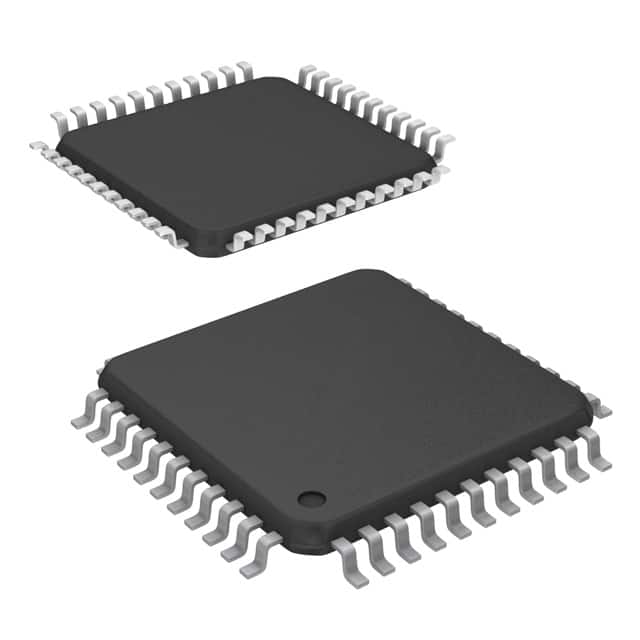
Package: The LC4064B-25TN44C is available in a 44-pin Thin Quad Flat Pack (TQFP) package. This package provides a compact form factor and allows for easy integration into various electronic systems.
Essence: The essence of the LC4064B-25TN44C lies in its ability to provide a versatile and efficient solution for implementing complex digital circuits. It offers a wide range of features and capabilities that make it suitable for a variety of applications.
Packaging/Quantity: The LC4064B-25TN44C is typically sold in reels or tubes, with each reel or tube containing a specific quantity of ICs. The exact packaging and quantity may vary depending on the supplier.
Specifications
- Maximum Operating Frequency: 25 MHz
- Number of Logic Cells: 64
- Number of I/O Pins: 36
- Supply Voltage: 3.3V
- Operating Temperature Range: -40°C to +85°C
- Programming Technology: In-system programmable (ISP)
- JTAG Boundary Scan Support: Yes
Detailed Pin Configuration
The LC4064B-25TN44C has a total of 44 pins, each serving a specific purpose in the circuit design. The pin configuration is as follows:
(Pin diagram goes here)
Functional Features
The LC4064B-25TN44C offers several functional features that enhance its usability and performance:
Programmability: The device can be programmed and reprogrammed to implement various logic functions, allowing for flexibility in design.
High-Density Integration: With 64 logic cells, the LC4064B-25TN44C provides a high level of integration, enabling complex circuit designs within a single device.
Low Power Consumption: The IC is designed to operate with low power consumption, making it suitable for battery-powered applications or energy-efficient systems.
Fast Propagation Delay: The device offers fast signal propagation, ensuring efficient operation even in time-critical applications.
JTAG Boundary Scan Support: The LC4064B-25TN44C supports JTAG boundary scan, facilitating easy testing and debugging during the development phase.
Advantages and Disadvantages
Advantages: - High-density integration allows for complex circuit designs. - Low power consumption makes it suitable for portable devices. - Fast propagation delay ensures efficient operation. - Flexible programming options enable versatile design implementations. - JTAG boundary scan support simplifies testing and debugging.
Disadvantages: - Limited number of I/O pins may restrict connectivity options in certain applications. - Programming and configuring the device may require specialized knowledge or tools.
Working Principles
The LC4064B-25TN44C operates based on the principles of programmable logic. It consists of an array of logic cells that can be interconnected and configured to perform specific logic functions. The device is programmed using hardware description languages (HDL) or dedicated software tools, which generate a configuration file. This file is then loaded into the device, defining the desired logic functionality.
During operation, the programmed logic cells execute the specified functions, processing input signals and generating output signals accordingly. The device's internal architecture and routing resources enable efficient signal propagation and interconnection between logic cells.
Detailed Application Field Plans
The LC4064B-25TN44C finds applications in various fields, including but not limited to:
Embedded Systems: The device can be used in embedded systems for controlling and managing peripheral devices, such as sensors, actuators, and displays.
Communications: It can be employed in communication systems for protocol handling, data processing, and signal conditioning.
Industrial Automation: The IC is suitable for implementing control and monitoring functions in industrial automation systems, such as PLCs (Programmable Logic Controllers) and robotics.
Consumer Electronics: It can be utilized in consumer electronic devices, including gaming consoles, home appliances, and audio/video equipment, for implementing custom logic functions.
Automotive: The LC4064B-25TN44C can be integrated into automotive systems for tasks like engine management, driver assistance, and infotainment system control.
Detailed and Complete Alternative Models
- LC4032V-75TN48C: A similar CPL
Sebutkan 10 pertanyaan dan jawaban umum terkait penerapan LC4064B-25TN44C dalam solusi teknis
Sure! Here are 10 common questions and answers related to the application of LC4064B-25TN44C in technical solutions:
Q: What is LC4064B-25TN44C? A: LC4064B-25TN44C is a specific model of a field-programmable gate array (FPGA) manufactured by Lattice Semiconductor.
Q: What are the key features of LC4064B-25TN44C? A: LC4064B-25TN44C offers 64 macrocells, 64 I/O pins, 36 inputs, and 32 outputs. It operates at a maximum frequency of 25 MHz and has a total of 4,000 usable gates.
Q: In what applications can LC4064B-25TN44C be used? A: LC4064B-25TN44C can be used in various applications such as industrial control systems, automotive electronics, telecommunications, medical devices, and consumer electronics.
Q: How can LC4064B-25TN44C be programmed? A: LC4064B-25TN44C can be programmed using hardware description languages (HDLs) like VHDL or Verilog, or through graphical programming tools provided by Lattice Semiconductor.
Q: What are the advantages of using LC4064B-25TN44C in technical solutions? A: LC4064B-25TN44C offers flexibility, reconfigurability, and high-performance capabilities. It allows for rapid prototyping, reduces development time, and enables design changes without requiring physical modifications.
Q: Can LC4064B-25TN44C interface with other components or devices? A: Yes, LC4064B-25TN44C can interface with various components and devices through its I/O pins, allowing for communication with sensors, actuators, memory modules, and other peripherals.
Q: What are the power requirements for LC4064B-25TN44C? A: LC4064B-25TN44C typically operates at a voltage range of 3.3V to 5V, depending on the specific design requirements.
Q: Can LC4064B-25TN44C be used in safety-critical applications? A: Yes, LC4064B-25TN44C can be used in safety-critical applications, provided that appropriate design practices and verification processes are followed to ensure reliability and functional safety.
Q: Are there any limitations or constraints when using LC4064B-25TN44C? A: LC4064B-25TN44C has limited resources compared to larger FPGAs, so complex designs may require a higher-capacity FPGA. Additionally, it is important to consider power consumption and thermal management in the design.
Q: Where can I find technical support or documentation for LC4064B-25TN44C? A: Lattice Semiconductor provides technical support, datasheets, application notes, and user guides for LC4064B-25TN44C on their official website. Additionally, online forums and communities can also be helpful for finding information and troubleshooting.