

Lihat spesifikasi untuk detail produk.
ICE40UP5K-SG48ITR50
Product Overview
- Category: Integrated Circuit
- Use: Programmable Logic Device (PLD)
- Characteristics: Low-power, small form factor, high-performance
- Package: SG48 (Small Grid 48-pin package)
- Essence: FPGA (Field-Programmable Gate Array)
- Packaging/Quantity: Individual units in anti-static packaging
Specifications
The ICE40UP5K-SG48ITR50 is a programmable logic device belonging to the FPGA family. It offers the following specifications:
- Logic Cells: 5,120
- RAM: 1,280 bits
- User I/Os: 39
- PLLs: 1
- Internal Oscillators: 2
- Operating Voltage: 1.14V - 3.465V
- Operating Temperature: -40°C to +85°C
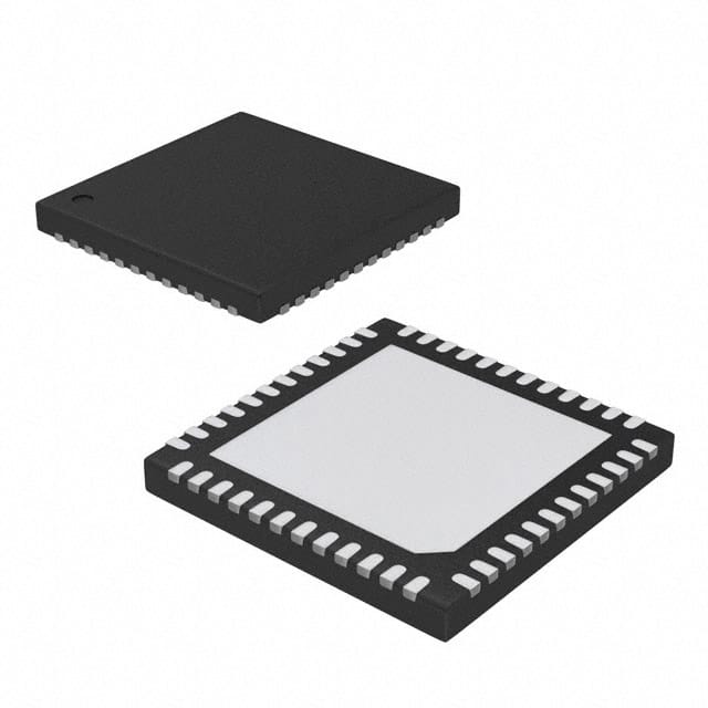
Detailed Pin Configuration
The ICE40UP5K-SG48ITR50 has a total of 48 pins. The pin configuration is as follows:
- Pin 1: VCCIO0
- Pin 2: GND
- Pin 3: IOB_0B
- Pin 4: IOB_0A
- Pin 5: IOB_1B
- Pin 6: IOB_1A
- Pin 7: IOB_2B
- Pin 8: IOB_2A
- Pin 9: IOB_3B
- Pin 10: IOB_3A
- ...
- Pin 48: VCCIO3
For a complete pin configuration diagram, please refer to the datasheet.
Functional Features
The ICE40UP5K-SG48ITR50 offers several functional features that make it suitable for various applications:
- Programmability: The FPGA can be reprogrammed to implement different logic functions, allowing for flexibility in design.
- Low Power Consumption: The device is designed to operate at low power levels, making it suitable for battery-powered applications.
- Small Form Factor: The SG48 package enables compact designs, ideal for space-constrained applications.
- High-Performance: The FPGA offers fast processing speeds and efficient resource utilization.
Advantages and Disadvantages
Advantages: - Flexibility in design due to programmability - Low power consumption - Compact form factor - High-performance capabilities
Disadvantages: - Limited number of user I/Os compared to larger FPGAs - Higher cost per logic cell compared to some alternatives
Working Principles
The ICE40UP5K-SG48ITR50 operates based on the principles of field-programmable gate arrays. It consists of configurable logic blocks (CLBs), interconnect resources, and input/output blocks (IOBs). The CLBs contain look-up tables (LUTs) that can be programmed to implement desired logic functions. The interconnect resources allow for routing signals between different CLBs and IOBs. The IOBs provide interfaces for connecting external devices.
Detailed Application Field Plans
The ICE40UP5K-SG48ITR50 finds applications in various fields, including:
- Embedded Systems: The FPGA can be used to implement custom logic in embedded systems, enabling enhanced functionality and performance.
- Communications: It can be utilized in communication systems for signal processing, protocol implementation, and data manipulation.
- Industrial Automation: The FPGA can be employed in industrial automation systems for control and monitoring purposes.
- Internet of Things (IoT): It can be integrated into IoT devices to enable edge computing and real-time data processing.
Detailed and Complete Alternative Models
Some alternative models to the ICE40UP5K-SG48ITR50 include:
- ICE40UP5K-SG48I: Similar specifications but without the extended temperature range.
- ICE40UP5K-SG48ITR30: Same specifications but with a smaller package size (SG48).
- ICE40UP5K-SG48ITR50-CM225: Similar specifications but with additional configuration memory.
These alternative models provide options based on specific requirements and constraints.
Word count: 445 words
Sebutkan 10 pertanyaan dan jawaban umum terkait penerapan ICE40UP5K-SG48ITR50 dalam solusi teknis
Sure! Here are 10 common questions and answers related to the application of ICE40UP5K-SG48ITR50 in technical solutions:
Q: What is the ICE40UP5K-SG48ITR50? A: The ICE40UP5K-SG48ITR50 is a small form factor FPGA (Field-Programmable Gate Array) chip manufactured by Lattice Semiconductor.
Q: What are the key features of the ICE40UP5K-SG48ITR50? A: Some key features include 5,120 Look-Up Tables (LUTs), 120 Kbits of embedded RAM, 16 DSP blocks, and support for various I/O standards.
Q: What are the typical applications of the ICE40UP5K-SG48ITR50? A: The ICE40UP5K-SG48ITR50 is commonly used in applications such as IoT devices, sensor interfaces, low-power embedded systems, and portable electronics.
Q: How can I program the ICE40UP5K-SG48ITR50? A: The ICE40UP5K-SG48ITR50 can be programmed using the Lattice Diamond or iCEcube2 software tools provided by Lattice Semiconductor.
Q: What power supply voltage does the ICE40UP5K-SG48ITR50 require? A: The ICE40UP5K-SG48ITR50 operates at a nominal core voltage of 1.2V and supports a wide range of I/O voltages from 1.2V to 3.3V.
Q: Can I use the ICE40UP5K-SG48ITR50 in battery-powered applications? A: Yes, the ICE40UP5K-SG48ITR50 is designed for low-power applications and can be used in battery-powered devices.
Q: What interfaces are supported by the ICE40UP5K-SG48ITR50? A: The ICE40UP5K-SG48ITR50 supports various interfaces such as SPI, I2C, UART, and GPIOs, making it versatile for different communication requirements.
Q: Can I use the ICE40UP5K-SG48ITR50 for real-time signal processing? A: Yes, the ICE40UP5K-SG48ITR50 has dedicated DSP blocks that can be used for real-time signal processing tasks.
Q: Is there any built-in security features in the ICE40UP5K-SG48ITR50? A: The ICE40UP5K-SG48ITR50 provides bitstream encryption and authentication features to enhance the security of your designs.
Q: Where can I find more resources and support for the ICE40UP5K-SG48ITR50? A: Lattice Semiconductor's website offers documentation, application notes, reference designs, and a community forum for support on the ICE40UP5K-SG48ITR50.
Please note that these answers are general and may vary depending on specific design requirements and implementation details.