

Lihat spesifikasi untuk detail produk.
ICE40LP384-CM49TR1K
Product Overview
Category
The ICE40LP384-CM49TR1K belongs to the category of programmable logic devices (PLDs).
Use
This product is primarily used for implementing digital logic circuits in various electronic systems.
Characteristics
- Programmable: The ICE40LP384-CM49TR1K can be configured to perform a wide range of functions.
- Low Power Consumption: It operates at low power levels, making it suitable for battery-powered devices.
- High Density: This PLD offers a high number of logic elements, allowing for complex designs.
- Small Form Factor: The package size and pin count are optimized for space-constrained applications.
Package
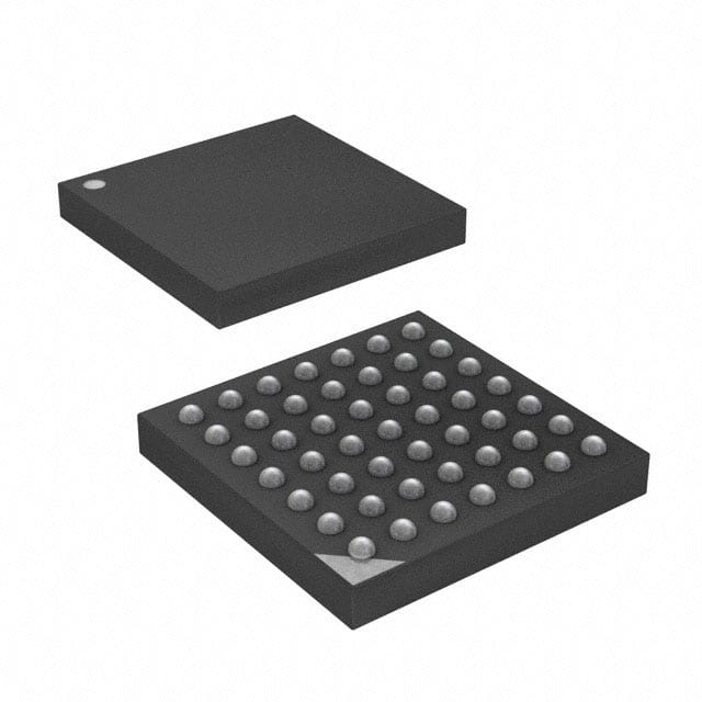
The ICE40LP384-CM49TR1K is available in a compact 49-ball chip-scale package (CM49).
Essence
The essence of this product lies in its ability to provide flexible and customizable digital logic functionality in a small form factor.
Packaging/Quantity
The ICE40LP384-CM49TR1K is typically supplied in tape and reel packaging, with a quantity of 1000 units per reel.
Specifications
- Logic Elements: 384
- User I/O Pins: 36
- Block RAM: 4.8 Kb
- Maximum Frequency: 100 MHz
- Operating Voltage: 1.2V
- Operating Temperature Range: -40°C to 85°C
Detailed Pin Configuration
The ICE40LP384-CM49TR1K has a total of 49 pins, each serving a specific purpose in the device's operation. For a detailed pin configuration diagram, please refer to the manufacturer's datasheet.
Functional Features
- Flexible Logic Implementation: The ICE40LP384-CM49TR1K allows users to implement a wide range of digital logic functions, including combinatorial and sequential circuits.
- On-Chip Memory: The built-in block RAM provides storage for data and intermediate results, enhancing the device's functionality.
- Clock Management: The PLD includes dedicated clock management resources, enabling precise timing control.
Advantages and Disadvantages
Advantages
- Versatility: The ICE40LP384-CM49TR1K can be programmed to perform various functions, making it suitable for diverse applications.
- Low Power Consumption: Its efficient design ensures minimal power usage, extending battery life in portable devices.
- Small Form Factor: The compact package size allows for integration into space-constrained designs.
Disadvantages
- Limited Resources: Compared to larger PLDs, the ICE40LP384-CM49TR1K has a relatively lower number of logic elements and I/O pins.
- Complexity: Programming and configuring the device may require specialized knowledge and tools.
Working Principles
The ICE40LP384-CM49TR1K operates based on the principles of field-programmable gate arrays (FPGAs). It consists of configurable logic blocks (CLBs), interconnect resources, and input/output blocks (IOBs). Users program the device by specifying the desired logic functions and interconnections using hardware description languages (HDLs) or graphical tools. Once programmed, the PLD executes the defined logic operations.
Detailed Application Field Plans
The ICE40LP384-CM49TR1K finds application in various fields, including:
- Consumer Electronics: It can be used in smartphones, tablets, and wearable devices for implementing custom logic functions.
- Industrial Automation: The PLD enables the implementation of control systems and signal processing algorithms in industrial equipment.
- Automotive Electronics: It can be utilized in automotive systems for functions like sensor interfacing and control logic.
- Internet of Things (IoT): The device is suitable for IoT applications, providing customizable logic for sensor data processing and connectivity.
Detailed and Complete Alternative Models
- ICE40LP384-CM36TR1K: Similar to the ICE40LP384-CM49TR1K, but with a 36-ball chip-scale package (CM36).
- ICE40LP1K-CM81TR1K: A larger variant with 1024 logic elements and an 81-ball chip-scale package (CM81).
- ICE40UP5K-SG48I: An ultra-low-power FPGA with 5280 logic elements and a 48-pin small-grid array package (SG48).
These alternative models offer different combinations of logic capacity, package size, and pin count, catering to diverse design requirements.
Word Count: 515 words
Sebutkan 10 pertanyaan dan jawaban umum terkait penerapan ICE40LP384-CM49TR1K dalam solusi teknis
Sure! Here are 10 common questions and answers related to the application of ICE40LP384-CM49TR1K in technical solutions:
Q1: What is ICE40LP384-CM49TR1K? A1: ICE40LP384-CM49TR1K is a low-power FPGA (Field-Programmable Gate Array) device manufactured by Lattice Semiconductor.
Q2: What are the key features of ICE40LP384-CM49TR1K? A2: Some key features of ICE40LP384-CM49TR1K include low power consumption, small form factor, high-performance fabric, and non-volatile configuration memory.
Q3: What are the typical applications of ICE40LP384-CM49TR1K? A3: ICE40LP384-CM49TR1K is commonly used in applications such as IoT devices, sensor interfaces, motor control, audio/video processing, and portable consumer electronics.
Q4: How does ICE40LP384-CM49TR1K achieve low power consumption? A4: ICE40LP384-CM49TR1K achieves low power consumption through its efficient architecture, power management features, and the ability to dynamically turn off unused resources.
Q5: Can ICE40LP384-CM49TR1K be programmed after deployment? A5: Yes, ICE40LP384-CM49TR1K can be reprogrammed even after it has been deployed in a system, allowing for flexibility and updates.
Q6: What tools are available for programming ICE40LP384-CM49TR1K? A6: Lattice Diamond software and iCEcube2 software are commonly used tools for designing, programming, and debugging ICE40LP384-CM49TR1K.
Q7: What is the maximum number of logic cells in ICE40LP384-CM49TR1K? A7: ICE40LP384-CM49TR1K has a maximum of 384 logic cells, which can be used to implement various digital functions.
Q8: Can ICE40LP384-CM49TR1K interface with other components or devices? A8: Yes, ICE40LP384-CM49TR1K supports various standard interfaces such as SPI, I2C, UART, and GPIOs, allowing it to communicate with other components or devices.
Q9: Does ICE40LP384-CM49TR1K support high-speed data processing? A9: Yes, ICE40LP384-CM49TR1K has dedicated high-speed I/O pins that can be used for high-speed data processing and communication.
Q10: Is there any documentation available for ICE40LP384-CM49TR1K? A10: Yes, Lattice Semiconductor provides datasheets, application notes, user guides, and reference designs for ICE40LP384-CM49TR1K, which can be accessed on their website.
Please note that the answers provided here are general and may vary depending on specific requirements and use cases.