

Lihat spesifikasi untuk detail produk.
ICE40LP1K-SWG16TR
Product Overview
- Category: Integrated Circuit
- Use: Programmable Logic Device (PLD)
- Characteristics: Low-power, Small form factor
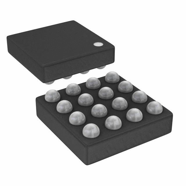
- Package: SWG16TR
- Essence: FPGA (Field-Programmable Gate Array)
- Packaging/Quantity: Tape and Reel, 2500 units per reel
Specifications
- Logic Cells: 1280
- User I/O Pins: 102
- Embedded Block RAM: 64 Kbits
- Operating Voltage: 1.14V - 1.26V
- Operating Temperature: -40°C to +85°C
- Speed Grade: Standard
Detailed Pin Configuration
The ICE40LP1K-SWG16TR has a total of 102 user I/O pins. These pins are configurable and can be used for various purposes such as input, output, or bidirectional communication. The pin configuration is as follows:
- Pin 1: GND
- Pin 2: IO_0
- Pin 3: IO_1
- ...
- Pin 101: IO_100
- Pin 102: VCC
Functional Features
- Low Power Consumption: The ICE40LP1K-SWG16TR is designed to operate at low power levels, making it suitable for battery-powered devices and energy-efficient applications.
- Small Form Factor: With its compact size and small package, this PLD can be easily integrated into space-constrained designs.
- High Flexibility: Being a programmable logic device, the ICE40LP1K-SWG16TR offers great flexibility in terms of design customization and reconfiguration.
- Fast Prototyping: The FPGA architecture allows for quick prototyping and iterative development, enabling faster time-to-market for new products.
Advantages and Disadvantages
Advantages: - Low power consumption - Small form factor - High flexibility in design - Fast prototyping capabilities
Disadvantages: - Limited logic cells compared to larger FPGAs - May require additional components for complex designs
Working Principles
The ICE40LP1K-SWG16TR is based on FPGA technology, which allows users to program the device according to their specific requirements. The PLD consists of configurable logic blocks, interconnects, and I/O pins. The user can define the functionality of these blocks by writing a hardware description language (HDL) code, which is then synthesized and implemented onto the FPGA. Once programmed, the device performs the desired functions based on the configured logic.
Detailed Application Field Plans
The ICE40LP1K-SWG16TR finds applications in various fields, including:
- Embedded Systems: It can be used in embedded systems to implement custom logic and interface with other components.
- Consumer Electronics: The low-power and small form factor make it suitable for portable devices such as smartphones, tablets, and wearables.
- IoT Devices: With its flexibility and low power consumption, the ICE40LP1K-SWG16TR can be utilized in IoT devices for sensor interfacing, data processing, and communication.
- Industrial Automation: It can be employed in industrial automation systems for control and monitoring purposes.
- Communications: The PLD can be used in communication equipment for signal processing, protocol implementation, and network interfaces.
Detailed and Complete Alternative Models
- ICE40LP4K-SWG32TR: Similar to the ICE40LP1K-SWG16TR but with 4 times the logic cells and 32 more user I/O pins.
- ICE40UP5K-SG48: A larger FPGA with 5280 logic cells and 39 user I/O pins, offering more resources for complex designs.
- MachXO2-7000HE-SWG324: An alternative PLD with 6864 logic cells and 324 user I/O pins, suitable for applications requiring higher density and I/O count.
These alternative models provide different options based on the specific requirements of the design.
In conclusion, the ICE40LP1K-SWG16TR is a low-power programmable logic device that offers flexibility, small form factor, and fast prototyping capabilities. It finds applications in various fields such as embedded systems, consumer electronics, IoT devices, industrial automation, and communications. While it has some limitations in terms of logic cell count, it provides an efficient solution for many design scenarios.
Sebutkan 10 pertanyaan dan jawaban umum terkait penerapan ICE40LP1K-SWG16TR dalam solusi teknis
Sure! Here are 10 common questions and answers related to the application of ICE40LP1K-SWG16TR in technical solutions:
Q1: What is the ICE40LP1K-SWG16TR? A1: The ICE40LP1K-SWG16TR is a low-power FPGA (Field-Programmable Gate Array) device manufactured by Lattice Semiconductor.
Q2: What are the key features of the ICE40LP1K-SWG16TR? A2: Some key features of the ICE40LP1K-SWG16TR include low power consumption, small form factor, high performance, and reprogrammability.
Q3: What are some typical applications of the ICE40LP1K-SWG16TR? A3: The ICE40LP1K-SWG16TR is commonly used in applications such as IoT devices, sensor interfaces, motor control, audio processing, and low-power embedded systems.
Q4: How does the ICE40LP1K-SWG16TR achieve low power consumption? A4: The ICE40LP1K-SWG16TR utilizes a combination of low-power design techniques, such as clock gating, power optimization algorithms, and dynamic power management, to minimize power consumption.
Q5: Can I program the ICE40LP1K-SWG16TR using popular programming languages like C or Python? A5: No, the ICE40LP1K-SWG16TR is programmed using Hardware Description Languages (HDLs) like Verilog or VHDL.
Q6: What development tools are available for programming the ICE40LP1K-SWG16TR? A6: Lattice Semiconductor provides the iCEcube2 software suite, which includes a graphical design environment and synthesis tools for programming the ICE40LP1K-SWG16TR.
Q7: Can the ICE40LP1K-SWG16TR be used in battery-powered devices? A7: Yes, the low power consumption of the ICE40LP1K-SWG16TR makes it suitable for battery-powered applications.
Q8: What is the maximum number of logic elements (LEs) available in the ICE40LP1K-SWG16TR? A8: The ICE40LP1K-SWG16TR has a maximum of 1280 logic elements (LEs).
Q9: Does the ICE40LP1K-SWG16TR support external memory interfaces? A9: Yes, the ICE40LP1K-SWG16TR supports various external memory interfaces like SPI, I2C, and UART.
Q10: Can the ICE40LP1K-SWG16TR be used for prototyping and development purposes? A10: Absolutely! The ICE40LP1K-SWG16TR is commonly used for prototyping and developing proof-of-concept designs due to its flexibility and reprogrammability.
Please note that these answers are general and may vary depending on specific use cases and requirements.