

Lihat spesifikasi untuk detail produk.
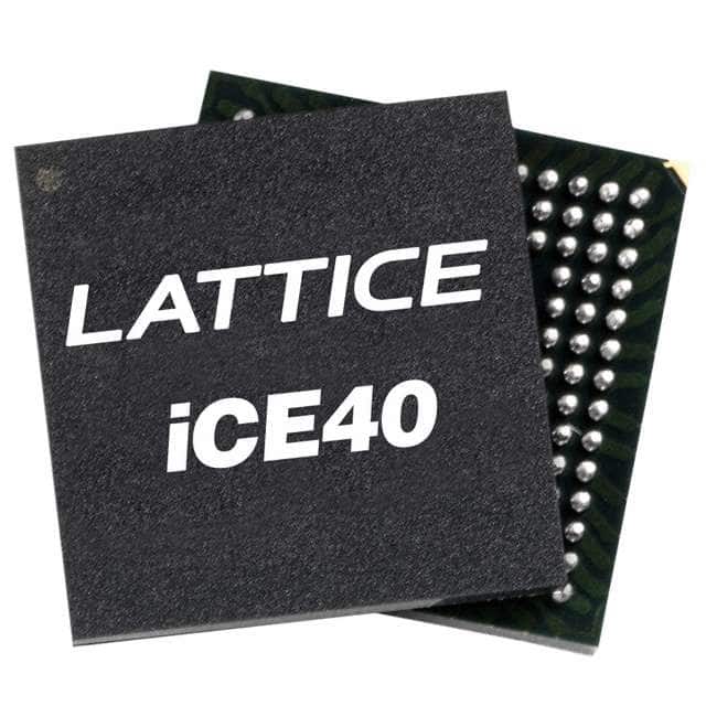
ICE40LP1K-CM36TR1K
Product Overview
- Category: Integrated Circuit
- Use: Programmable Logic Device (PLD)
- Characteristics: Low power consumption, small form factor, high performance
- Package: CM36TR1K
- Essence: The ICE40LP1K-CM36TR1K is a programmable logic device designed for various applications that require low power consumption and high performance. It is commonly used in electronic devices such as smartphones, tablets, and IoT devices.
- Packaging/Quantity: The ICE40LP1K-CM36TR1K is available in the CM36TR1K package and is typically sold in reels or trays.
Specifications
- Logic Cells: 1,000
- Operating Voltage: 1.2V
- Operating Temperature Range: -40°C to 85°C
- Speed Grade: Standard (6)
- I/O Pins: 36
- Memory Blocks: 8
- Embedded RAM: 64 Kbits
- Clock Management: PLLs, DLLs
- Configuration Memory: Non-volatile Flash
Detailed Pin Configuration
The ICE40LP1K-CM36TR1K has a total of 36 I/O pins. These pins are used for input/output connections with other components in the system. The pin configuration is as follows:
- Pin 1: VCCIO
- Pin 2: GND
- Pin 3: IO0
- Pin 4: IO1
- Pin 5: IO2
- Pin 6: IO3
- Pin 7: IO4
- Pin 8: IO5
- Pin 9: IO6
- Pin 10: IO7
- Pin 11: IO8
- Pin 12: IO9
- Pin 13: IO10
- Pin 14: IO11
- Pin 15: IO12
- Pin 16: IO13
- Pin 17: IO14
- Pin 18: IO15
- Pin 19: IO16
- Pin 20: IO17
- Pin 21: IO18
- Pin 22: IO19
- Pin 23: IO20
- Pin 24: IO21
- Pin 25: IO22
- Pin 26: IO23
- Pin 27: IO24
- Pin 28: IO25
- Pin 29: IO26
- Pin 30: IO27
- Pin 31: IO28
- Pin 32: IO29
- Pin 33: IO30
- Pin 34: IO31
- Pin 35: IO32
- Pin 36: IO33
Functional Features
- Low Power Consumption: The ICE40LP1K-CM36TR1K is designed to operate with low power consumption, making it suitable for battery-powered devices and energy-efficient applications.
- Small Form Factor: With its compact size and package, the ICE40LP1K-CM36TR1K can be easily integrated into space-constrained electronic designs.
- High Performance: Despite its small size, the ICE40LP1K-CM36TR1K offers high performance and can handle complex logic functions efficiently.
Advantages and Disadvantages
Advantages: - Low power consumption - Small form factor - High performance - Versatile programmable logic device
Disadvantages: - Limited number of I/O pins - Not suitable for applications requiring a large number of logic cells
Working Principles
The ICE40LP1K-CM36TR1K is based on the field-programmable gate array (FPGA) technology. It consists of programmable logic cells, memory blocks, clock management circuitry, and configuration memory. The device can be programmed to implement various logic functions by configuring the interconnections between logic cells.
During operation, the configuration memory stores the programming information, which is loaded into the device upon power-up or reconfiguration. The clock management circuitry provides clock signals for synchronous operations within the device.
Detailed Application Field Plans
The ICE40LP1K-CM36TR1K is widely used in various electronic applications, including:
- Smartphones and Tablets: The low power consumption and small form factor of the ICE40LP1K-CM36TR1K make it suitable for integration into mobile devices, enabling efficient processing and control functions.
- Internet of Things (IoT) Devices: With its high performance and low power consumption,
Sebutkan 10 pertanyaan dan jawaban umum terkait penerapan ICE40LP1K-CM36TR1K dalam solusi teknis
Sure! Here are 10 common questions and answers related to the application of ICE40LP1K-CM36TR1K in technical solutions:
Q1: What is ICE40LP1K-CM36TR1K? A1: ICE40LP1K-CM36TR1K is a low-power FPGA (Field-Programmable Gate Array) device manufactured by Lattice Semiconductor. It offers 1,000 Look-Up Tables (LUTs) and is commonly used in various technical solutions.
Q2: What are the key features of ICE40LP1K-CM36TR1K? A2: Some key features of ICE40LP1K-CM36TR1K include low power consumption, small form factor, high performance, and reprogrammability.
Q3: What are the typical applications of ICE40LP1K-CM36TR1K? A3: ICE40LP1K-CM36TR1K is commonly used in applications such as IoT devices, sensor interfaces, motor control, audio/video processing, and general-purpose digital logic.
Q4: How can I program ICE40LP1K-CM36TR1K? A4: ICE40LP1K-CM36TR1K can be programmed using Lattice Diamond or iCEcube2 software tools provided by Lattice Semiconductor. These tools allow you to design and implement your desired functionality on the FPGA.
Q5: What is the power consumption of ICE40LP1K-CM36TR1K? A5: The power consumption of ICE40LP1K-CM36TR1K depends on the specific design and usage scenario. However, it is known for its low power characteristics, making it suitable for battery-powered applications.
Q6: Can I interface ICE40LP1K-CM36TR1K with other components or devices? A6: Yes, ICE40LP1K-CM36TR1K supports various interfaces such as SPI, I2C, UART, and GPIOs. This allows you to easily interface it with other components or devices in your technical solution.
Q7: What is the maximum operating frequency of ICE40LP1K-CM36TR1K? A7: The maximum operating frequency of ICE40LP1K-CM36TR1K depends on the specific design and implementation. However, it can typically operate at frequencies up to 100 MHz.
Q8: Can I use ICE40LP1K-CM36TR1K for real-time signal processing? A8: Yes, ICE40LP1K-CM36TR1K can be used for real-time signal processing tasks. Its high-performance capabilities and reprogrammability make it suitable for such applications.
Q9: Is ICE40LP1K-CM36TR1K suitable for low-cost solutions? A9: Yes, ICE40LP1K-CM36TR1K is known for its cost-effectiveness. It offers a good balance between performance and price, making it suitable for low-cost technical solutions.
Q10: Are there any development boards available for ICE40LP1K-CM36TR1K? A10: Yes, Lattice Semiconductor provides development boards specifically designed for ICE40LP1K-CM36TR1K, such as the iCEstick Evaluation Kit. These boards allow you to prototype and test your designs using the FPGA.