

Lihat spesifikasi untuk detail produk.
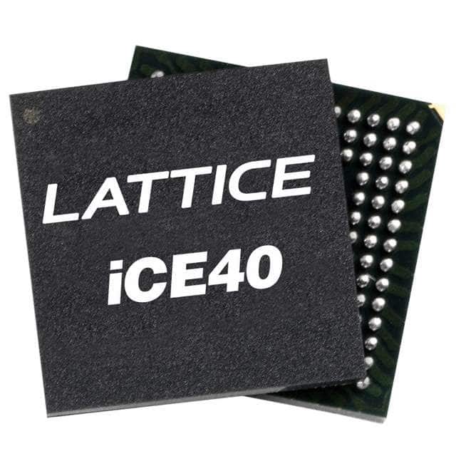
ICE40LM2K-CM36TR1K
Product Overview
- Category: Integrated Circuit
- Use: Programmable Logic Device (PLD)
- Characteristics: Low power consumption, small form factor, high performance
- Package: CM36TR1K
- Essence: The ICE40LM2K-CM36TR1K is a programmable logic device designed for low-power applications. It offers high performance and flexibility in a compact package.
- Packaging/Quantity: Available in CM36TR1K package, quantity varies based on supplier.
Specifications
- Logic Elements: 2000
- RAM Bits: 64 Kbits
- User I/O Pins: 36
- Operating Voltage: 1.2V
- Operating Temperature Range: -40°C to 85°C
- Speed Grade: Standard
Detailed Pin Configuration
The ICE40LM2K-CM36TR1K has a total of 36 user I/O pins. These pins can be configured as inputs or outputs based on the application requirements. The pin configuration is as follows:
- Pin 1: VCCIO
- Pin 2: GND
- Pin 3: IO0
- Pin 4: IO1
- Pin 5: IO2
- Pin 6: IO3
- Pin 7: IO4
- Pin 8: IO5
- Pin 9: IO6
- Pin 10: IO7
- Pin 11: IO8
- Pin 12: IO9
- Pin 13: IO10
- Pin 14: IO11
- Pin 15: IO12
- Pin 16: IO13
- Pin 17: IO14
- Pin 18: IO15
- Pin 19: IO16
- Pin 20: IO17
- Pin 21: IO18
- Pin 22: IO19
- Pin 23: IO20
- Pin 24: IO21
- Pin 25: IO22
- Pin 26: IO23
- Pin 27: IO24
- Pin 28: IO25
- Pin 29: IO26
- Pin 30: IO27
- Pin 31: IO28
- Pin 32: IO29
- Pin 33: IO30
- Pin 34: IO31
- Pin 35: IO32
- Pin 36: IO33
Functional Features
- Low Power Consumption: The ICE40LM2K-CM36TR1K is designed to operate at low power levels, making it suitable for battery-powered devices and energy-efficient applications.
- High Performance: With 2000 logic elements and 64 Kbits of RAM, this PLD offers high performance and can handle complex logic functions.
- Small Form Factor: The compact CM36TR1K package allows for easy integration into space-constrained designs.
Advantages and Disadvantages
Advantages
- Low power consumption
- High performance
- Small form factor
- Flexible pin configuration
Disadvantages
- Limited number of user I/O pins (36)
- May not be suitable for applications requiring a large number of I/O connections
Working Principles
The ICE40LM2K-CM36TR1K is based on the field-programmable gate array (FPGA) technology. It consists of configurable logic blocks (CLBs), interconnect resources, and I/O blocks. The CLBs can be programmed to implement various logic functions, allowing for customization based on the application requirements. The interconnect resources enable communication between different CLBs, while the I/O blocks provide connectivity to external devices.
Detailed Application Field Plans
The ICE40LM2K-CM36TR1K is suitable for a wide range of applications, including:
- Internet of Things (IoT) devices
- Wearable technology
- Consumer electronics
- Industrial automation
- Medical devices
Detailed and Complete Alternative Models
- ICE40LP2K-CM36TR1K: Similar to ICE40LM2K-CM36TR1K but with 4000 logic elements.
- ICE40UP5K-CM36TR1K: Offers higher performance with 5280 logic elements and additional features.
These alternative models provide options with varying capabilities to suit different application requirements.
Word count: 511
Sebutkan 10 pertanyaan dan jawaban umum terkait penerapan ICE40LM2K-CM36TR1K dalam solusi teknis
Sure! Here are 10 common questions and answers related to the application of ICE40LM2K-CM36TR1K in technical solutions:
Q1: What is the ICE40LM2K-CM36TR1K? A1: The ICE40LM2K-CM36TR1K is a low-power FPGA (Field-Programmable Gate Array) device manufactured by Lattice Semiconductor.
Q2: What are the key features of the ICE40LM2K-CM36TR1K? A2: Some key features include 3840 Look-Up Tables (LUTs), 36 kilobits of embedded memory, low power consumption, and support for various I/O standards.
Q3: What are some typical applications of the ICE40LM2K-CM36TR1K? A3: The ICE40LM2K-CM36TR1K is commonly used in applications such as IoT devices, sensor interfaces, motor control, portable medical devices, and more.
Q4: How can I program the ICE40LM2K-CM36TR1K? A4: The ICE40LM2K-CM36TR1K can be programmed using Lattice Diamond or iCEcube2 design software, which supports Verilog and VHDL languages.
Q5: What is the power consumption of the ICE40LM2K-CM36TR1K? A5: The power consumption of the ICE40LM2K-CM36TR1K depends on the specific design and operating conditions, but it is known for its low power characteristics.
Q6: Can the ICE40LM2K-CM36TR1K interface with other components? A6: Yes, the ICE40LM2K-CM36TR1K supports various I/O standards, including LVCMOS, LVTTL, and LVDS, allowing it to interface with a wide range of components.
Q7: What is the maximum operating frequency of the ICE40LM2K-CM36TR1K? A7: The maximum operating frequency of the ICE40LM2K-CM36TR1K depends on the specific design and implementation, but it can typically reach frequencies in the tens or hundreds of megahertz range.
Q8: Can I use the ICE40LM2K-CM36TR1K for real-time applications? A8: Yes, the ICE40LM2K-CM36TR1K can be used for real-time applications, provided that the design meets the timing requirements and constraints of the application.
Q9: Does the ICE40LM2K-CM36TR1K support non-volatile configuration? A9: No, the ICE40LM2K-CM36TR1K does not have built-in non-volatile memory. It requires an external configuration device, such as an SPI flash, to store the configuration bitstream.
Q10: Are there any development boards available for the ICE40LM2K-CM36TR1K? A10: Yes, Lattice Semiconductor offers development boards like the iCE40 UltraPlus Breakout Board, which can be used for prototyping and evaluation of the ICE40LM2K-CM36TR1K.
Please note that these answers are general and may vary depending on specific design requirements and implementation details.