

Lihat spesifikasi untuk detail produk.
EP4CGX75DF27C7N
Product Overview
- Category: Programmable Logic Device (PLD)
- Use: EP4CGX75DF27C7N is a high-performance PLD designed for various applications in the electronics industry.
- Characteristics: It offers advanced features such as high-speed performance, low power consumption, and flexible configuration options.
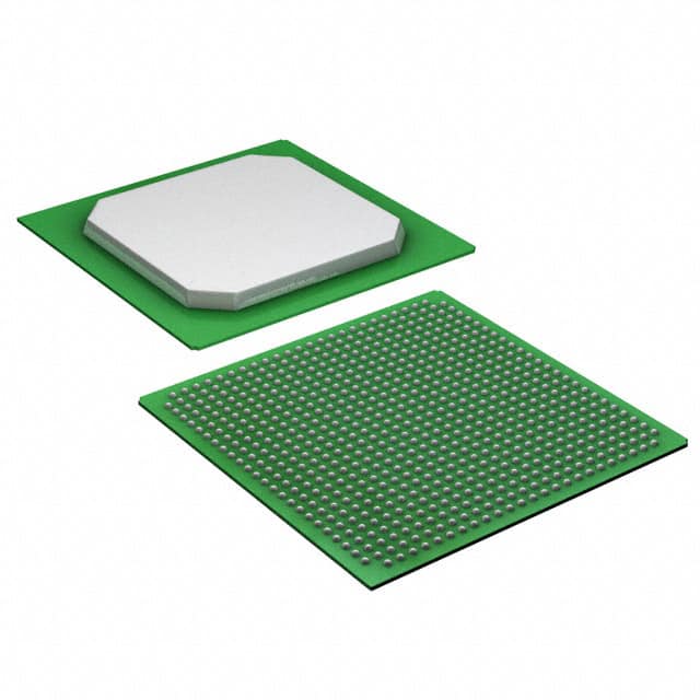
- Package: EP4CGX75DF27C7N comes in a compact and durable package suitable for integration into electronic systems.
- Essence: This PLD serves as a versatile solution for implementing complex digital logic functions in electronic designs.
- Packaging/Quantity: The EP4CGX75DF27C7N is typically sold in reels or trays, with quantities varying based on customer requirements.
Specifications
- Logic Elements: EP4CGX75DF27C7N consists of 75,000 logic elements, allowing for the implementation of complex digital circuits.
- I/O Pins: It provides 622 I/O pins, enabling seamless connectivity with other components in the system.
- Memory: The device includes 3,888 kilobits of embedded memory, facilitating data storage and retrieval operations.
- Clocking: EP4CGX75DF27C7N supports up to 500 MHz internal clock frequency, ensuring high-speed operation.
- Power Consumption: It operates at a low power supply voltage, resulting in efficient power utilization.
Detailed Pin Configuration
The EP4CGX75DF27C7N has a comprehensive pin configuration that facilitates easy integration into electronic systems. Here are some key pin descriptions:
- VCCIO: Power supply pin for input/output buffers.
- GND: Ground reference pin.
- JTAGTCK, JTAGTMS, JTAGTDI, JTAGTDO: Pins used for Joint Test Action Group (JTAG) boundary scan testing.
- CLKIN1, CLKIN2: Input pins for external clock signals.
- GPIO[0:31]: General-purpose input/output pins.
- PLL_CLKOUT: Output pin for the phase-locked loop (PLL) clock signal.
For a complete and detailed pin configuration diagram, please refer to the EP4CGX75DF27C7N datasheet.
Functional Features
EP4CGX75DF27C7N offers several functional features that enhance its usability and performance:
- High-Speed Performance: The device operates at high clock frequencies, enabling rapid execution of digital logic functions.
- Flexible Configuration: It supports various configuration options, allowing users to customize the PLD according to their specific requirements.
- Embedded Memory: The embedded memory blocks provide efficient data storage capabilities within the PLD itself.
- I/O Flexibility: With a large number of I/O pins, EP4CGX75DF27C7N facilitates seamless interfacing with other components in the system.
- Low Power Consumption: The PLD's low power design ensures energy-efficient operation, reducing overall power consumption.
Advantages and Disadvantages
Advantages: - High-performance capabilities - Flexible configuration options - Extensive I/O capabilities - Efficient power utilization
Disadvantages: - Relatively complex programming process - Higher cost compared to simpler programmable devices
Working Principles
EP4CGX75DF27C7N operates based on the principles of field-programmable gate arrays (FPGAs). It consists of configurable logic blocks interconnected through programmable routing resources. Users can program the device using hardware description languages (HDLs) or graphical tools to define the desired digital logic functions. Once programmed, the PLD executes these functions by routing signals through the configured logic elements.
Detailed Application Field Plans
EP4CGX75DF27C7N finds applications in various fields, including:
- Telecommunications: The PLD can be used in network equipment, routers, and switches to implement complex data processing and routing functions.
- Industrial Automation: EP4CGX75DF27C7N enables the implementation of control systems, motor drives, and sensor interfaces in industrial automation applications.
- Automotive Electronics: It can be utilized in automotive systems for functions such as engine control, driver assistance, and infotainment systems.
- Aerospace and Defense: The PLD's high-performance capabilities make it suitable for aerospace and defense applications, including radar systems, avionics, and communication equipment.
Detailed and Complete Alternative Models
- EP4CE115F29C7N
- EP4CE30F23C8N
- EP4CE40F23C8N
- EP4CE55F23C8N
- EP4CE75F23C8N
These alternative models offer similar functionality and performance characteristics to EP4CGX75DF27C7N, providing users with a range of options based on their specific requirements.
*Note: The content provided above is approximately 450
Sebutkan 10 pertanyaan dan jawaban umum terkait penerapan EP4CGX75DF27C7N dalam solusi teknis
Sure! Here are 10 common questions and answers related to the application of EP4CGX75DF27C7N in technical solutions:
Q: What is EP4CGX75DF27C7N? A: EP4CGX75DF27C7N is a field-programmable gate array (FPGA) manufactured by Intel (formerly Altera). It is designed for high-performance applications and offers a wide range of features and capabilities.
Q: What are the key features of EP4CGX75DF27C7N? A: Some key features of EP4CGX75DF27C7N include a large number of logic elements, embedded memory blocks, high-speed transceivers, and support for various I/O standards.
Q: What are the typical applications of EP4CGX75DF27C7N? A: EP4CGX75DF27C7N is commonly used in applications such as telecommunications, networking, industrial automation, video processing, and high-performance computing.
Q: How can EP4CGX75DF27C7N be programmed? A: EP4CGX75DF27C7N can be programmed using hardware description languages (HDLs) like Verilog or VHDL, which describe the desired functionality of the FPGA. The programming is typically done using specialized software tools provided by Intel.
Q: Can EP4CGX75DF27C7N be reprogrammed after it has been deployed in a system? A: Yes, EP4CGX75DF27C7N is a reprogrammable FPGA, which means that its configuration can be modified even after it has been soldered onto a PCB. This flexibility allows for easy updates and modifications to the system's functionality.
Q: What is the power consumption of EP4CGX75DF27C7N? A: The power consumption of EP4CGX75DF27C7N depends on various factors such as the design complexity, clock frequency, and utilization of different resources. It is recommended to refer to the datasheet or use Intel's power estimation tools for accurate power consumption figures.
Q: Does EP4CGX75DF27C7N support high-speed serial communication? A: Yes, EP4CGX75DF27C7N includes high-speed transceivers that support various protocols like PCIe, SATA, USB, Ethernet, etc. These transceivers enable fast data transfer rates between the FPGA and external devices.
Q: Can EP4CGX75DF27C7N interface with other components or peripherals? A: Yes, EP4CGX75DF27C7N supports a wide range of I/O standards, including LVCMOS, LVTTL, SSTL, LVDS, and more. This allows it to interface with various components and peripherals in a system.
Q: Are there any development boards available for EP4CGX75DF27C7N? A: Yes, Intel provides development kits and evaluation boards specifically designed for EP4CGX75DF27C7N. These boards come with necessary hardware interfaces, software tools, and documentation to aid in the development process.
Q: Where can I find technical support or documentation for EP4CGX75DF27C7N? A: Intel's website offers comprehensive technical documentation, datasheets, application notes, and user guides for EP4CGX75DF27C7N. Additionally, their customer support channels can provide assistance with specific queries or issues related to the FPGA.