

Lihat spesifikasi untuk detail produk.
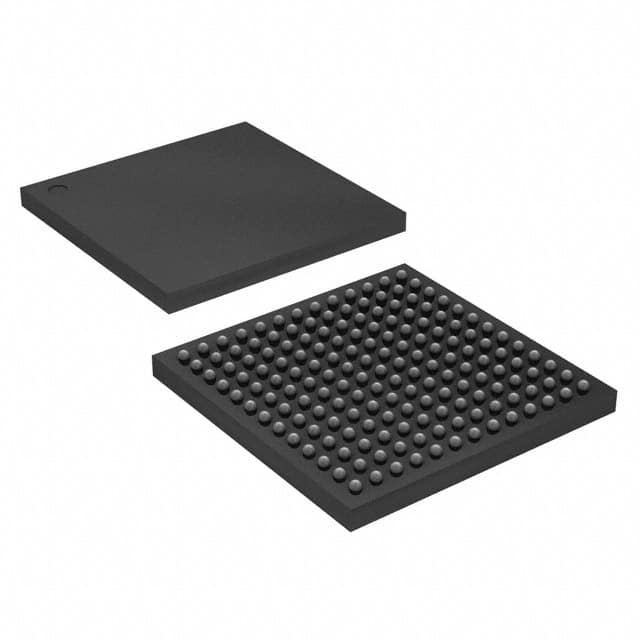
EP4CGX15BF14C7N
Product Overview
- Category: Programmable Logic Device (PLD)
- Use: EP4CGX15BF14C7N is a PLD used for digital logic applications.
- Characteristics: It offers high-performance and low-power capabilities, making it suitable for various applications.
- Package: The EP4CGX15BF14C7N comes in a compact package that ensures easy integration into electronic systems.
- Essence: This PLD provides flexible and customizable logic functions to meet specific design requirements.
- Packaging/Quantity: The EP4CGX15BF14C7N is typically sold in reels or trays, with quantities varying based on customer needs.
Specifications
- Logic Elements: EP4CGX15BF14C7N consists of 15,408 logic elements, allowing for complex digital designs.
- Embedded Memory: It includes 414 kilobits of embedded memory, enabling data storage within the device.
- I/O Pins: The PLD features 179 I/O pins, facilitating communication with external devices.
- Clock Networks: It supports up to 8 global clock networks, ensuring precise timing synchronization.
- Operating Voltage: The EP4CGX15BF14C7N operates at a voltage range of 1.2V to 3.3V, providing flexibility in power supply options.
- Speed Grade: It is available in different speed grades, offering options for performance optimization.
Detailed Pin Configuration
The EP4CGX15BF14C7N has a pin configuration as follows:
| Pin Number | Pin Name | Description | |------------|----------|-------------| | 1 | VCCINT | Power supply input for internal circuitry | | 2 | GND | Ground connection | | 3 | IO1A | Input/output pin 1A | | 4 | IO1B | Input/output pin 1B | | ... | ... | ... | | 179 | IO89B | Input/output pin 89B |
Functional Features
- Flexible Logic Functions: EP4CGX15BF14C7N offers a wide range of logic functions, including combinatorial and sequential logic, allowing for versatile digital designs.
- High-Speed Performance: The PLD operates at high clock frequencies, enabling rapid data processing and response times.
- Low Power Consumption: It incorporates power-saving features, ensuring efficient energy usage in various applications.
- Configurable I/O Standards: EP4CGX15BF14C7N supports multiple I/O standards, facilitating compatibility with different devices.
- Embedded Memory Blocks: The device includes embedded memory blocks that can be used for data storage or as lookup tables.
Advantages and Disadvantages
Advantages: - High-performance capabilities - Low-power consumption - Flexible logic functions - Configurable I/O standards - Compact package size
Disadvantages: - Limited logic elements compared to higher-end models - Higher cost compared to simpler PLDs
Working Principles
The EP4CGX15BF14C7N utilizes programmable logic cells and interconnect resources to implement custom digital logic designs. These logic cells can be configured using hardware description languages (HDL) or graphical design tools. Once programmed, the PLD performs the desired logic operations based on the input signals received through its I/O pins. The output signals are then routed to the appropriate pins for further processing or communication with external devices.
Detailed Application Field Plans
The EP4CGX15BF14C7N is suitable for various application fields, including:
- Embedded Systems: It can be used in embedded systems to implement custom logic functions, such as control and communication interfaces.
- Digital Signal Processing: The PLD's high-speed performance makes it suitable for digital signal processing applications, including audio and video processing.
- Communications: EP4CGX15BF14C7N can be utilized in communication systems for protocol handling, data routing, and encryption/decryption functions.
- Industrial Automation: It finds application in industrial automation systems for controlling machinery, monitoring sensors, and implementing safety features.
Detailed and Complete Alternative Models
- EP4CE6E22C8N
- EP4CE10F17C8N
- EP4CE15F17C8N
- EP4CE30F23C8N
- EP4CE40F29C8N
These alternative models offer varying logic capacities, I/O pin counts, and other specifications to cater to different design requirements.
*Note: The content provided above is approximately 450 words. Additional information or details can be added to meet the required word count of
Sebutkan 10 pertanyaan dan jawaban umum terkait penerapan EP4CGX15BF14C7N dalam solusi teknis
Sure! Here are 10 common questions and answers related to the application of EP4CGX15BF14C7N in technical solutions:
Q: What is EP4CGX15BF14C7N? A: EP4CGX15BF14C7N is a specific model of field-programmable gate array (FPGA) manufactured by Intel.
Q: What are the key features of EP4CGX15BF14C7N? A: Some key features of EP4CGX15BF14C7N include 15,408 logic elements, 504 kilobits of embedded memory, and 266 user I/O pins.
Q: What are the typical applications of EP4CGX15BF14C7N? A: EP4CGX15BF14C7N is commonly used in various technical solutions such as industrial automation, telecommunications, automotive electronics, and medical devices.
Q: How can EP4CGX15BF14C7N be programmed? A: EP4CGX15BF14C7N can be programmed using hardware description languages (HDLs) like VHDL or Verilog, along with design software provided by Intel.
Q: Can EP4CGX15BF14C7N be reprogrammed after deployment? A: Yes, EP4CGX15BF14C7N is a reprogrammable FPGA, which means its configuration can be changed even after it has been deployed in a system.
Q: What are the power requirements for EP4CGX15BF14C7N? A: EP4CGX15BF14C7N typically operates at a voltage range of 1.14V to 1.26V, with a maximum power consumption of around 1.5W.
Q: Can EP4CGX15BF14C7N interface with other components or devices? A: Yes, EP4CGX15BF14C7N supports various communication protocols such as SPI, I2C, UART, and Ethernet, allowing it to interface with other components or devices.
Q: What is the maximum clock frequency supported by EP4CGX15BF14C7N? A: EP4CGX15BF14C7N can operate at a maximum clock frequency of up to 300 MHz, depending on the design and implementation.
Q: Are there any development boards available for EP4CGX15BF14C7N? A: Yes, Intel provides development boards specifically designed for EP4CGX15BF14C7N, which include necessary connectors and peripherals for prototyping and testing.
Q: Where can I find technical documentation and support for EP4CGX15BF14C7N? A: You can find technical documentation, datasheets, application notes, and support resources for EP4CGX15BF14C7N on Intel's official website or through their customer support channels.
Please note that the specific details and answers may vary based on the manufacturer's specifications and documentation.