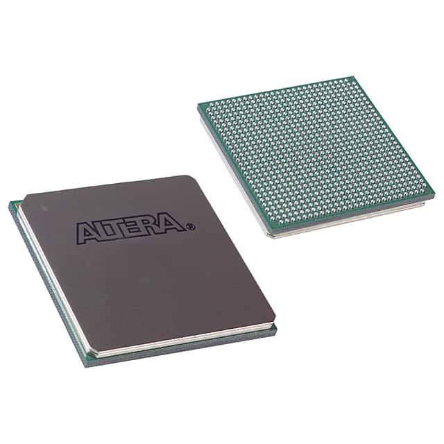
Lihat spesifikasi untuk detail produk.

EP3SE80F780C2N
Product Overview
- Category: Programmable Logic Device (PLD)
- Use: EP3SE80F780C2N is a high-performance PLD designed for various applications in the field of digital logic design and implementation.
- Characteristics:
- High-speed performance
- Large capacity
- Low power consumption
- Flexible configuration options
- Package: EP3SE80F780C2N comes in a compact and durable package, ensuring easy handling and protection during transportation and installation.
- Essence: EP3SE80F780C2N is an essential component in electronic systems that require complex logic functions to be implemented efficiently.
- Packaging/Quantity: Each package contains one EP3SE80F780C2N device.
Specifications
- Logic Elements: 80,000
- Embedded Memory: 1,152 Kbits
- Maximum User I/O Pins: 622
- Clock Networks: 12
- PLLs: 4
- Maximum Operating Frequency: 500 MHz
- Voltage Range: 1.14V to 1.26V
- Power Consumption: 0.5W (typical)
Detailed Pin Configuration
The EP3SE80F780C2N has a total of 622 user I/O pins, which are configurable based on the specific application requirements. These pins can be used for input, output, or bidirectional purposes. The pin configuration is as follows:
- Pin 1: VCCIO
- Pin 2: GND
- Pin 3: IO_0
- Pin 4: IO_1
- ...
- Pin 621: IO_620
- Pin 622: IO_621
Functional Features
- High-Speed Performance: EP3SE80F780C2N offers fast operation speeds, making it suitable for applications that require real-time processing and high-speed data transfer.
- Large Capacity: With 80,000 logic elements and 1,152 Kbits of embedded memory, this PLD can handle complex designs and accommodate a significant amount of data.
- Low Power Consumption: EP3SE80F780C2N is designed to minimize power consumption, ensuring energy efficiency in electronic systems.
- Flexible Configuration Options: The device supports various configuration options, allowing designers to customize the logic functions according to their specific requirements.
Advantages and Disadvantages
Advantages: - High-performance capabilities - Large capacity for complex designs - Low power consumption - Flexible configuration options
Disadvantages: - Relatively higher cost compared to lower-end PLDs - Steeper learning curve for beginners due to its advanced features
Working Principles
EP3SE80F780C2N operates based on the principles of programmable logic. It consists of configurable logic blocks (CLBs), interconnect resources, embedded memory, and I/O pins. The CLBs can be programmed to implement various logic functions, while the interconnect resources enable the connection between different blocks. The embedded memory provides storage for data, and the I/O pins facilitate communication with external devices.
Detailed Application Field Plans
EP3SE80F780C2N finds applications in various fields, including:
- Telecommunications: Used in network routers, switches, and communication equipment for high-speed data processing.
- Industrial Automation: Employed in control systems, robotics, and factory automation for efficient and reliable operation.
- Automotive Electronics: Integrated into automotive control units, infotainment systems, and driver assistance systems for enhanced functionality.
- Aerospace and Defense: Utilized in avionics, radar systems, and military-grade electronics for critical operations and data processing.
Detailed and Complete Alternative Models
- EP3SE110F780C2N: A higher-capacity version of EP3SE80F780C2N with 110,000 logic elements.
- EP3SE40F780C2N: A lower-capacity version of EP3SE80F780C2N with 40,000 logic elements.
- EP3SE160F780C2N: A higher-capacity version of EP3SE80F780C2N with 160,000 logic elements.
These alternative models offer different capacity options to cater to diverse design requirements.
Word count: 550 words
Sebutkan 10 pertanyaan dan jawaban umum terkait penerapan EP3SE80F780C2N dalam solusi teknis
Sure! Here are 10 common questions and answers related to the application of EP3SE80F780C2N in technical solutions:
Q: What is EP3SE80F780C2N? A: EP3SE80F780C2N is a specific model of Field-Programmable Gate Array (FPGA) manufactured by Intel.
Q: What are the key features of EP3SE80F780C2N? A: Some key features of EP3SE80F780C2N include high-performance logic fabric, embedded memory blocks, DSP blocks, and various I/O interfaces.
Q: What are the typical applications of EP3SE80F780C2N? A: EP3SE80F780C2N is commonly used in applications such as telecommunications, industrial automation, aerospace, defense, and high-performance computing.
Q: How can EP3SE80F780C2N be programmed? A: EP3SE80F780C2N can be programmed using Hardware Description Languages (HDLs) like VHDL or Verilog, which describe the desired functionality of the FPGA.
Q: Can EP3SE80F780C2N be reprogrammed after initial programming? A: Yes, EP3SE80F780C2N is a reprogrammable FPGA, allowing for flexibility in design changes or updates.
Q: What tools are available for designing with EP3SE80F780C2N? A: Intel provides Quartus Prime software, which includes design entry, synthesis, simulation, and programming tools specifically for EP3SE80F780C2N.
Q: What is the power consumption of EP3SE80F780C2N? A: The power consumption of EP3SE80F780C2N depends on the specific design and usage, but it typically ranges from a few watts to tens of watts.
Q: Can EP3SE80F780C2N interface with other components or devices? A: Yes, EP3SE80F780C2N supports various I/O standards and interfaces like PCIe, Ethernet, USB, SPI, I2C, and more, allowing it to communicate with external devices.
Q: Are there any limitations or considerations when using EP3SE80F780C2N? A: Some considerations include power supply requirements, thermal management, timing constraints, and the need for proper grounding and decoupling techniques.
Q: Where can I find additional resources or support for EP3SE80F780C2N? A: Intel provides documentation, application notes, reference designs, and an online community forum where you can find additional resources and support for EP3SE80F780C2N.
Please note that the answers provided here are general and may vary depending on the specific requirements and use cases. It is always recommended to refer to the official documentation and consult with experts for accurate and detailed information.

