Lihat spesifikasi untuk detail produk.

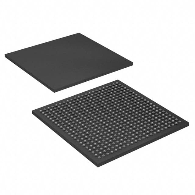
EP3SE50F484I4N
Product Overview
- Category: Field Programmable Gate Array (FPGA)
- Use: EP3SE50F484I4N is a high-performance FPGA designed for various applications in the electronics industry.
- Characteristics: This FPGA offers advanced features such as high-speed performance, low power consumption, and reconfigurability.
- Package: The EP3SE50F484I4N comes in a 484-pin FineLine BGA package.
- Essence: It is a key component used to implement digital logic circuits in electronic systems.
- Packaging/Quantity: The EP3SE50F484I4N is typically sold individually or in small quantities.
Specifications
- Logic Elements: The FPGA contains 50,000 equivalent logic elements.
- Memory: It has 1,152 Kbits of embedded memory.
- Clock Management: The device includes up to 8 phase-locked loops (PLLs) for clock management.
- I/O Interfaces: It supports various I/O standards, including LVCMOS, LVTTL, and differential signaling standards.
- Operating Voltage: The EP3SE50F484I4N operates at a voltage range of 1.2V to 1.5V.
- Operating Temperature: It can operate within a temperature range of -40°C to 100°C.
Pin Configuration
The EP3SE50F484I4N has a detailed pin configuration with 484 pins. Please refer to the manufacturer's datasheet for the complete pinout information.
Functional Features
- High-Speed Performance: The FPGA offers fast processing capabilities, making it suitable for applications that require real-time data processing.
- Reconfigurability: The EP3SE50F484I4N can be reprogrammed multiple times, allowing for flexibility in design and functionality.
- Low Power Consumption: It is designed to minimize power consumption, making it energy-efficient.
- Versatile I/O Interfaces: The FPGA supports a wide range of I/O standards, enabling seamless integration with other electronic components.
Advantages and Disadvantages
Advantages: - High-performance processing capabilities - Reconfigurable nature allows for flexibility in design - Low power consumption for energy efficiency - Versatile I/O interfaces for easy integration
Disadvantages: - Complex programming and configuration process - Limited availability of alternative models - Higher cost compared to other programmable logic devices
Working Principles
The EP3SE50F484I4N operates based on the principles of digital logic circuits. It consists of configurable logic blocks (CLBs), interconnects, memory elements, and I/O interfaces. The CLBs can be programmed to implement various logic functions, while the interconnects provide routing paths between different components. The memory elements store data temporarily, and the I/O interfaces enable communication with external devices.
Application Field Plans
The EP3SE50F484I4N finds applications in various fields, including: 1. Telecommunications: Used in network routers, switches, and base stations for high-speed data processing. 2. Industrial Automation: Employed in control systems, robotics, and machine vision applications for real-time processing and control. 3. Automotive Electronics: Integrated into automotive control units for advanced driver assistance systems (ADAS) and infotainment systems. 4. Aerospace and Defense: Utilized in radar systems, avionics, and military communication equipment for reliable and high-performance operation.
Alternative Models
While the EP3SE50F484I4N is a popular FPGA model, there are alternative options available from other manufacturers. Some notable alternatives include: - Xilinx Virtex-7 XC7VX485T FPGA - Intel Cyclone V GT EP5CGXFF7 FPGA - Lattice ECP5-85 FPGA
These alternative models offer similar features and performance, providing options for designers based on their specific requirements.
Word count: 445 words
Sebutkan 10 pertanyaan dan jawaban umum terkait penerapan EP3SE50F484I4N dalam solusi teknis
Sure! Here are 10 common questions and answers related to the application of EP3SE50F484I4N in technical solutions:
Q: What is EP3SE50F484I4N? A: EP3SE50F484I4N is a specific model of Field-Programmable Gate Array (FPGA) manufactured by Intel.
Q: What are the key features of EP3SE50F484I4N? A: Some key features include 50,000 logic elements, 1,288 embedded memory blocks, and support for various I/O standards.
Q: What are the typical applications of EP3SE50F484I4N? A: EP3SE50F484I4N is commonly used in applications such as industrial automation, telecommunications, automotive systems, and high-performance computing.
Q: How can EP3SE50F484I4N be programmed? A: EP3SE50F484I4N can be programmed using Hardware Description Languages (HDLs) like VHDL or Verilog, along with design software provided by Intel.
Q: Can EP3SE50F484I4N be reprogrammed after initial programming? A: Yes, EP3SE50F484I4N is a reprogrammable FPGA, allowing for flexibility in design iterations and updates.
Q: What are the power requirements for EP3SE50F484I4N? A: The power requirements vary depending on the specific design and usage scenario. It is recommended to refer to the datasheet for detailed information.
Q: Does EP3SE50F484I4N support communication protocols? A: Yes, EP3SE50F484I4N supports various communication protocols such as UART, SPI, I2C, Ethernet, and PCIe.
Q: Can EP3SE50F484I4N interface with external devices? A: Yes, EP3SE50F484I4N has multiple I/O pins that can be used to interface with external devices like sensors, displays, and memory modules.
Q: Are there any development boards available for EP3SE50F484I4N? A: Yes, Intel provides development boards specifically designed for EP3SE50F484I4N, which include necessary connectors and peripherals for prototyping and testing.
Q: Where can I find technical documentation and support for EP3SE50F484I4N? A: You can find technical documentation, datasheets, reference designs, and support resources on the official Intel website or community forums dedicated to FPGA development.

